Continue to Site

Welcome to EDAboard.com

Welcome to our site! EDAboard.com is an international Electronics Discussion Forum focused on EDA software, circuits, schematics, books, theory, papers, asic, pld, 8051, DSP, Network, RF, Analog Design, PCB, Service Manuals... and a whole lot more! To participate you need to register. Registration is free. Click here to register now.

[SOLVED] label/pin on a net with a differet name DRC error

Status
Not open for further replies.

preethi19

Full Member level 5
Joined
Jun 30, 2014
Messages
273
Helped
0
Reputation
0
Reaction score
1
Trophy points
16
Activity points
3,474
Hi initially wen doing layout in cadence i used VSS and gnd on the same substrate and got the error "label/pin on a net with differnet name". I got the suggestion to add a dnw layer and isolate the two. I put VSS within the dnw and outside gnd and the error was cleared. But now to get the output from a transistor's drain i need to drive it through a load resistor of 1K. And so i connect one end of resistor to drain of transistor and place a output pin 'Iout' on that metal. The other end of resistor is grounded. And in layout resistor is in a n well with a bulk layer which i gave it to VDD. Now i am getting the same above error between 'gnd' and 'Iout'.

Vss and gnd i can understand the input potential to same p-substrate. but why between gnd and iout??? Can anyone plsss tell me how to correct this. I wasn't sure if the method was right but i tried using dnw around resistor.. Still didnt work.. Pls help!!!!
 
Last edited:
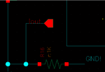
I was able to solve the above error and get 0 errors in DRC but then wen i run LVS the netlists dont match between the extraction and schematic giving me few errors that no of nets dont match etc. But then wen i leave the above error like that without correcting it and when i run LVS then netlists match with all nets equal and no other errors in LVS but the above error remains pending in the DRC. Could anyone kindly help. Tried many things but still couldn't get it working.

The error is in the Iout pin. Normally the output is driven through a load resistor. So while doing simulation i select the Rplus terminal of the resistor to obtain the output.

Untitled.png

But now i connect a wire in between the transistor drain and the resistor's terminal. And did the same in schematic. Pls let me know wer the correction is needed. Thank you!!!
 

I'm a little confused. You were able to fix your original LVS problem but in doing so you created a DRC error? You then fixed your DRC error but created a LVS problem? What is/was the DRC error?
 

Status
Not open for further replies.

Part and Inventory Search

Welcome to EDABoard.com

Sponsor

Back
Top