Continue to Site

Welcome to EDAboard.com

Welcome to our site! EDAboard.com is an international Electronics Discussion Forum focused on EDA software, circuits, schematics, books, theory, papers, asic, pld, 8051, DSP, Network, RF, Analog Design, PCB, Service Manuals... and a whole lot more! To participate you need to register. Registration is free. Click here to register now.

High voltage input cascaded buck converter

Status
Not open for further replies.
T

treez

Guest
Hello,
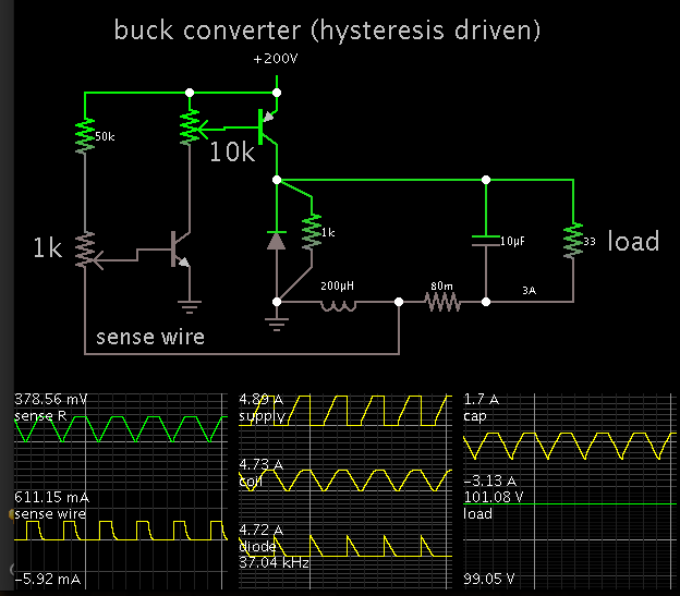
We have to do a non-isolated SMPS for vin=120v to 400v, and vout = 100v, pout=300w.
There is a “known” way to do this involving two cascaded synchronous buck stages. The upstream stage works either in DCM or in resonant mode so as to provide a lower voltage bus for the downstream buck, so that the downstream buck suffers less switching loss.
The upstream buck stage suffers low switching loss due to being in either resonant mode or in DCM (zero fet current at turn on).
Both buck hi-side fets are literally driven from the same output of a single current mode controller (eg ucc28c4x series). Current sense transformers and high side gate drive transformers thrown in as required. Only the output of the downstream buck is regulated.
Do you know more detail of this “known” method?
 

I'm not seeing why two stages would be advantageous.
 
  • Like
Reactions: treez

    T

    Points: 2
    Helpful Answer Positive Rating
Hello,
Do you know if there is any problem with just putting the buck converters in parallel, with just the one controller commanding the duty cycle of each fet? (ltspice simulation and pdf schem attached)

There should be no sharing issue like this?
 

Attachments

  • Parallel Bucks.pdf
    17.3 KB · Views: 152
  • Parallel Bucks.txt
    7.6 KB · Views: 97
  • Parallel Bucks 400vin.txt
    7.6 KB · Views: 121
Last edited by a moderator:

In your schematic there is no way to ensure that the two stages share the load current equally. Interleaved converters must be controlled with CMC on each phase, and there are many controllers which implement this.
 
  • Like
Reactions: treez

    T

    Points: 2
    Helpful Answer Positive Rating
Thanks though those controllers cannot withstand the 170degC ambient that we are dealing with here.
There is just one error amplifier between the two parallel bucks, and the duty cycle for each fet is the same....the current throughput in each parallel buck will surely be pretty much the same?
 

In your schematic there is no way to ensure that the two stages share the load current equally. Interleaved converters must be controlled with CMC on each phase, and there are many controllers which implement this.
They can be expected to achieve a fair sharing by operating then with equal duty cycle (or some gate signal, if you don't place importance on interleaving). Inductor DCR and MOSFET Rdson tend to balance the load current.

Surely precise current control is preferable.
 
  • Like
Reactions: treez

    T

    Points: 2
    Helpful Answer Positive Rating
Is there any possibility of placing this buck regulator out of the hole, and using remote voltage sensing to control the regulating action ?
 

If its for a universal "world" power supply that is not an unreasonable range.
Low limit voltage in Japan might be 85v RMS, high limit voltage in Australia might be 265v RMS.

Peak rectify that, and you see something like 120 dc to 375v dc.
 

This is a far cry from being a solution, but it illustrates what sort of control circuit is possible with a 2-transistor Sziklai pair. Hysteresis is achieved with a sense resistor in a strategic position.

Simulator values are adjusted to get 100V output with 200V supply. It is not regulated as yet. Output voltage varies with supply voltage.

The NPN is biased at 611 mA, which will destroy it. Some re-designing is needed.


Please may I offer more info, we think this dual cascaded buck converter is bogus...do you agree?

...We have received a 300w dual cascaded buck converter (vin=120vdc to 400vdc; vout=100vdc) that does not work, we are being asked to make it work, but I think this circuit is a bogus design…please offer your opinion?
(its for a 170degc ambient measurement while drilling application.)

Please find attached the ltspice simulation of it and the pdf schematic. For comparison, it is simulated alongside a fictitious single stage buck for the same spec.

As you know, a cascade of SMPS’s would rarely be more efficient than a single SMPS, since the power is processed twice. In this case, with the high Vin, it was possible that the goal was to reduce the “power density in any single semiconductor”…in this case, the switching FET of the upstream buck, due to the fact that it suffers a large switching loss, due to the high vin of 400vdc.

However, when compared to a single stage buck converter, this is not necessarily the case at all. Please find attached a comparitive simulation of the cascaded bucks, and a single stage buck SMPS.

The upstream buck of the cascade is in DCM when at 400vin, the “advantage” of the cascade is seen in that the VDS of the upstream FET swings fully from 400V to 0V. (That is, it swings either side of its (intermediary) output voltage. This creates the opportunity to switch the fet on when its vds is zero. However, this would require a zero-crossing detector circuit, and no such thing exists here, and with the semiconductor limitation of MWD, this isn’t a likely possibility.
As such, its entirely possible that the fet could be switched on with its vds voltage being fully 400v. –In such a case, the circuit would have no advantage over a single stage buck converter….and would be more inefficient.

If we look at the comparitive simulation, it shows that the vds of the fet in the single stage only swings about 200v down from 400v, thus there is not such a possibility for reduced switch-on loss…however, the possibility would exist. The problem again is that there is no minimum drain voltage detection.

Also, demonstrated in the simulation is a dual “parallel” buck smps, which is, as you know, more efficient than a cascade or single buck. As you know, the parallel current paths mean a halving of conduction losses. There would not be sharing issues if they both use the one controller as per the sim.

……………………………………………………………………
Other situations.

PNP turn off:
Also noted was that the PNP turn off circuit had a 10R resistor connected Base-emitter. As you know, this could potentially result in damage to the PNP turn-off as Vbe max is about 5v. As you know, the PNP turn-off is best connected with the diode Base-emitter.

Current sense transformer:
This is wound on an E-type core with mating halves. As you know, GDT’s are best wound bifilar on torroids using TIW if necessary.

Dead time
The RT/CT combination of the UCC28C43 is 59600R/2n2. This give a minimum off time of just 500ns. This is going to require a very high reset voltage for the CST. As you know, the CT cap should be increased and the RT reduced, since the discharge current in the ucc18c43 is 8.4mA.
This will also help the situation with the hi side fet drives.

Sync fets
Two sync fets, and that complex drive circuitry, seems excessive, since the worst case diode av. current in the single stage circuit is 2.2A, -could be done with a few parallel sic (PTC) diodes.

Slope compensation
The lower 120vin to 100vout situation would need slope compensation if done in CCM. However, I cannot see any slope compensation at the first viewing. With the low frequency setting, high vin, and low inductor values, it looks as if (deep) DCM was opted for, but this has the disadvantage of needing bigger inductor if peak current is too high, etc etc. It makes you wonder if they didn’t just opt for DCM because of the greater ease of feedback loop compensation.

Is this dual cascaded buck converter bogus?

the actual schematic has a 11.1uh inductor for the downstream buck inductor, but this would give ridiculously high peak current when vin=400vdc, I therefore made the downstream inductor bigger for this simulation.
 

Attachments

  • Buck comparison schematic1.pdf
    23.1 KB · Views: 143
  • Buck comparison1.txt
    11.9 KB · Views: 110

Hello,
So, this is essentially the “barking mad” circuit that we have been told to get working on the bench in the lab. I managed to get it working in this LTspice simulation attached, but only by changing the downstream buck’s inductor to 220uH from 11.1uH. I also added slope compensation, and changed the control chip from a 50% maximum ucc28c44 to a 95% max duty cycle ucc28c43. Also, due to the extreme ringing with the intermediary rail in between the two bucks, I had to add a large (470n) integrating capacitor to the feedback loop so as to stabilise it.

The switching frequency is 20khz and so the gate drive transformer had to have its L(mag) increased from 400uH to 8mH…otherwise the magnetising current destroys the operation of the hi-side gate drive circuit.

However, do you agree that this circuit is “barking mad”, and would better be done by a single buck stage, or two bucks in parallel (as in post#3 above)?

Do you agree?
 

Attachments

  • Dual cascaded buck converters.pdf
    28.5 KB · Views: 173
  • Dual Cascaded bucks.txt
    15 KB · Views: 97

Despite this SMPS being very poor, because of being 2 bucks in cascade rather than parallel.......strangely, from 120Vin to 100Vout , and in CCM current mode, it needs no slope compensdation...do you know why?
LTspice sim and pdf schem supplied
 

Attachments

  • Cascaded bucks _no slope comp.pdf
    19.8 KB · Views: 173
  • Cascaded bucks _no slope comp.txt
    8.5 KB · Views: 102

If there is a high amount of magnetising current, this gives the same effect as slope compensation, also for a large output L less slope comp is needed...
 
  • Like
Reactions: treez

    T

    Points: 2
    Helpful Answer Positive Rating
Thanks, as you know, slope compensation is required as per (slope comp ramp) / (off time ramp of inductor) = 1-0.18/D.

The duty cycle is 0.91 when vin = 120v and vout = 100v (because the ‘intermediary’ voltage is 109v).

Even with a very large inductor(s), the slope compensation ramp needed would still normally be very significant, …though as you can see in the simulation in post above (post #13) , there is absolutely no slope compensation whatsoever, and yet there is utterly no subharmonic oscillation…..there is something special going on here.
Do you know why no slope compensation at all was needed in the simulation in post #13 above? (schematic also shown)
 

If there is a high amount of magnetising current, this gives the same effect as slope compensation
Thanks for offering an answer, but I believe that you have mistaken this for a two transistor forward or some such, (I understand exactly why you haven't read my above posts properly and apologise for my oft-times laborious preceeding explanations in the above posts) because this post concerns a dual cascaded buck converter, and in this case the magnetising current doesn't offer a slope compensation ramp.......there are current sense transformers in this post's subject, but as you know, the magnetising current in the secondary of these actually subtracts from the ramp...so its worse than nothing as regards slope compensation.

Anybody know why the dual cascaded buck (seen in post #13) with ccm current mode, and 90% duty cycle needs no slope compensation?
 

For a straight buck converter, the smaller the L the higher the peaks on the trapezoidal current, which is like having a large magnetising current (on a push pull) - this offers the only explanation of stability at high duty cycle.

- - - Updated - - -

Also - your circuit in the pdf shows that you are using slope comp, Q1 R14 into the Isense pin...
 
  • Like
Reactions: treez

    T

    Points: 2
    Helpful Answer Positive Rating
Thankyou, i apologise as i have I uploaded the wrong ltspice simulation and schematic in post #13 above, here is the correct ones....(they show the dual cascaded buck converter with 90% duty cyle and not needing slope compensation)
Once again, why is no slope compensation needed for the dual cascaded buck converter in current mode, 90% duty cycle?
 

Attachments

  • Cascaded bucks _no slope comp_2.txt
    8.1 KB · Views: 100
  • Cascaded bucks _no slope comp_2.pdf
    19.4 KB · Views: 178

Um, a simulation will often work perfectly at a point that is inherently unstable in the real world, unless you introduce a perturbation to knock it away from where it sits, if you modulate the Vin, you might well see the sub-harmonic oscillation caused by no slope comp in current mode, a lot of effort goes into sims to make them converge on an operating point, rather than diverge away from...
 
  • Like
Reactions: treez

    T

    Points: 2
    Helpful Answer Positive Rating
Thanks, very true, just today simulated the exact same ltspice circuit on the work PC instead and it suffers bad subharmonic oscillation and needs the slope compensation.
 

Status
Not open for further replies.

Part and Inventory Search

Welcome to EDABoard.com

Sponsor

Back
Top