Continue to Site

Welcome to EDAboard.com

Welcome to our site! EDAboard.com is an international Electronics Discussion Forum focused on EDA software, circuits, schematics, books, theory, papers, asic, pld, 8051, DSP, Network, RF, Analog Design, PCB, Service Manuals... and a whole lot more! To participate you need to register. Registration is free. Click here to register now.

LTSpice model for grid tied invertor

Status
Not open for further replies.

DanyR

Member level 3
Joined
Aug 23, 2015
Messages
67
Helped
6
Reputation
12
Reaction score
6
Trophy points
8
Location
Nieuwpoort, Belgium
Activity points
677
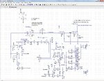
LTSpice simple model for grid tied invertor

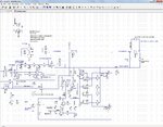
Hi, I am learning to work with LTSpice and I am also very interested about the "how" of grid tied invertors, so I decided to make a very simplified and basic circuit diagram in LtSpice that could be simulated.

Reference see https://www.edaboard.com/threads/345807/.

The starting points were:
- the invertor deliveres a constant current to the grid/load of 2A peak (AC)
- the current is in phase with the grid voltage
- the grid is always connected and stable

The circuit presented lacks a lot of stuff that should be added later:
- the PWM drive of the output transistors (power stage) + addition of the PWM filter of course
- circuitry to startup/connect/disconnect the invertor in a safe way
- stabilisation of the AC reference voltage (Vin in the diagram)
- a way to make the constant output current changeable
- feed and adapt the power curcuit (and others if necessary) so that it can cope with a grid voltage of 230Vac.
- safety circuitry e.g. in case the grid gets disconnected etc...

In the circuit diagram only a grid voltage of 10V peak was used (V5).
The load (of e.g. the whole household) is represented by RLoad and draws 0.5A AC peak. This means that, when the invertor delivers 2A AC peak, the grid (V5) will be fed with 1.5A peak AC.

How it works:

The AC reference voltage is made with R11 and R12, and is stable since the VGrid (V5) does not change in this simulation. Additionally the derivation of the reference from the grid with a simple R voltage divider ensures the current delivered out of the invertor will be in phase with the grid voltage.

A series resistor in the output of the invertor (R2) is used to measure the current delivered by the invertor. The voltage across it (0.01V/A) is amplified 100 times with B1 (voltage controlled voltage source), wich gives an 1V/A sensivity at comparator U4. The latter compares that current derived voltage with the reference voltage...
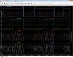
Grid_Invertor_asc.jpgGrid_Invertor_raw.jpg
 

Hi,

In above post one of the items to be ameliorated was the reference voltage of 2V peak AC. Shown as above its value depends on the value of the grid voltage.

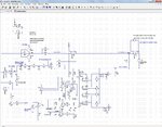
Here is a replacement for the simple divider as shown in the above post:
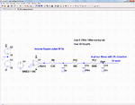
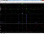
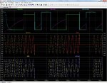
Ref_Voltage_Invertor_asc.gif Ref_Voltage_invertor_raw.gif
The output of the circuit (Out1 in the diagram) is still in phase with the grid voltage (V1 in the diagram) but its amplitude is solely defined by the supply voltage of the op-amp U1 and the filter after it.
The op-amp makes a square wave with a phase shift of 180 degrees with repect to the grid voltage, and the filter itself also causes 180 degress phase shift, which results in an output in phase with the input.

Please provide comments if you are interested or see some problems (I forgot to ask this in the previous post).
I would like to extend the model with all featuring needed for a "real" grid tied invertor.
Thanks in advance.
 

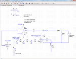
Adding the above reference voltage circuit to the invertor circuit gives the following:
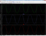
Invertor_3_asc.gifInvertor_3_raw.gif
I had to add a 1 ohm resistor (R7) in the output of the power stage to prevent huge currents (+ instability) during startup of the circuit. The reason for this is that the reference voltage is not stable let's say the first 50 millisecs.
Later a switch between the power stage and the grid (mains) will be added that connects both after all is stable.
The Vref filter delivers a bit more than 2Vpeak, so the current delivered by the invertor will be slightly bigger than 2A peak, see the diagrams.
 

I had to add a 1 ohm resistor (R7) in the output of the power stage to prevent huge currents (+ instability) during startup of the circuit. The reason for this is that the reference voltage is not stable let's say the first 50 millisecs.
Later a switch between the power stage and the grid (mains) will be added that connects both after all is stable.
A real grid tied inverter would surely have a disconnection switch and connect to the grid through an inductor, which is part of the pwm frequency filter.
 
  • Like
Reactions: DanyR

    DanyR

    Points: 2
    Helpful Answer Positive Rating
A real grid tied inverter would surely have a disconnection switch and connect to the grid through an inductor, which is part of the pwm frequency filter.
Yes indeed. Those parts have still to be added. In the mean time this problem is "solved" by adding R7.

For a list of things to to: see the first post in this thread.

Thanks for the review and the comment! :p
 

Hi, the following has been added:

- a switch (S2 in the diagram) to be able to separate the invertor from the grid. If the switch is open (invertor not connected to the grid) the system stabilises its output ("Out" in the diagram to the same voltage as the grid (represented by V5 in the diagram) so that the closing of the switch will be smooth. The stabilisation is done with U2 via S4). If the switch is closed (invertor connected to the grid) the system stabilises its output current to 2 A peak AC (as before). This is done with U4 and S3.

- The circuitry to control the switch state. This is done with a bistable multivib: Q3 and Q4. Its "Control" output being high will switch on S2 and S3 and swicth off S4.
The bistable multivib is bought in the "Off" state ("Control" = low) by an error in the mains voltage, which is monitored by U3, U5, U6 and U7. Basically here the peak voltages of the mains are checked here (over and under voltage).
If the mains voltage deviates too much from the normal one the line "ErrVmains" becomes high and resets the bistable multivibs "Control" output too low, resulting in a switch off.
The basic idea is that, when the mains gets disconnected the output voltage of the invertor will become too high (with little or no lead), or too low (wigh high load).
If the mains voltage becomes Ok again the bistable multivib is "set" again via D8, D4 and R20. This is the "retry" circuit. The retry frequency (or retry wait time) is defined by R26, C7 and D8.

In the circuit diagram there is also S1 added. This one is there only to simulate the grid disconnection, it is not part of the invertor circuit diagram.

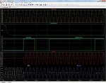
Below the circuit diagram and the "traces":
Invertor_4_raw.jpgInvertor_4_asc.jpg

There is one reamining problem I can not solve:

if the current through RLoad is approximately the same as the current delivered by the invertor (meaning the current delivered by the grid is near to zero), then of course disconnecting of the grid can not be seen by the invertor. The output voltage stays within the limits, and even its shape stays sinusoidal (thanks to the filter at the output of U1).

In this case the invertor will not be switched off by S2, it will stay connected to the grid, with safety problems as consequence. Also when the grid comes back there will occur a short circuit...

Anyone any ideas? Thanks in advance!
 
Last edited:

An extra question: how to measure the phase margin of the circuit in the above post in LTSpice? There are 2 feedback paths (working mutually exclusive): one via U1 and one via U2.

Thanks in advance!
 

More important questions are ;
What is your inverter source impedance and desired effect from load regulation? Z(f) ratio of load/source
What is response to step load , reactive pulsed step load( e.g. cap bridge rectifier) and a short circuit fault?
What is response to a disturbance? e.g. 1,10 us 4kV, line transient or half cycle drop out.
What changes are necessary to prevent failure?
What is startup and transfer characteristic with inductive load?
 
  • Like
Reactions: DanyR

    DanyR

    Points: 2
    Helpful Answer Positive Rating
More important questions are ;
What is your inverter source impedance and desired effect from load regulation? Z(f) ratio of load/source
What is response to step load , reactive pulsed step load( e.g. cap bridge rectifier) and a short circuit fault?
What is response to a disturbance? e.g. 1,10 us 4kV, line transient or half cycle drop out.
What changes are necessary to prevent failure?
What is startup and transfer characteristic with inductive load?
Hi, thanks for the extensive response. Indeed I still have to add a lot of things, especially those that have to do with failiures and disturbances. I am aware of that, but first I want to have the theoretical model right.

One important point (I think): you talk about e.g. "inductive load" and "Step load", but there is no such thing. The only load is the grid itself, which is (theoretically) not changable (a voltage source which has a zero ohm internal resistor). In fact the invertor sees a load impedance of zero ohm. All other things (such as RLoad) are actually not "seen" by the invertor. Of course things change if the grid is of low quality (e.h. high internal resistance/impedance) or the grid gets disconnected.

The latter error condition is detected by measuring the output voltage of the invertor. If it is out of bounds the flip flop Q3/Q4 will disconnect the invertor from the grid/load (S1). Also a short circuit fault should be covered this way.

But: for the circuit as it is now, how can I make a phase margin analysis in LTSpice while the invertor is still "working" (without disturbing its normal behaviour)?
 
Last edited:

I beg to differ but the loop impedance includes load and source. So When I say step load that includes power source and ground. So in effect it is a step change in supply voltage and phase with respect to the grid . Nothing is 0 ohms and 0 phase error but perhaps close compared to your source, even so, include transmission line impedance. Grid is typically 5% line regulation worst case and 5% generation meaning 10% variations in voltage but Zo to sub for short circuit may be up to 20kA. THis implies a source impedance.
DT's are usually 2~8%pu.

Search Youtube for videos on how to do Bode Plots.
 
  • Like
Reactions: DanyR

    DanyR

    Points: 2
    Helpful Answer Positive Rating
I beg to differ but the loop impedance includes load and source. So When I say step load that includes power source and ground. So in effect it is a step change in supply voltage and phase with respect to the grid . Nothing is 0 ohms and 0 phase error but perhaps close compared to your source, even so, include transmission line impedance. Grid is typically 5% line regulation worst case and 5% generation meaning 10% variations in voltage but Zo to sub for short circuit may be up to 20kA. THis implies a source impedance.
DT's are usually 2~8%pu.
Thanks. Of course you are right about the "reality" of the grid behaviour. I surely have to take them into account. At this moment the "grid" in my LTSpice simulation (V5) has no internal impedance whatsoever, and has no changing (nor amplitude, not phase) charactristics. So, steady as a rock... :) Making this more realistic in the simulation is for later I am afraid.

Also my source impedance (I assume you mean V+ and V-) is theoritically an ideal one, and of course this will surely not be true... Making this more realistic in the simulation is also for later I am afraid.

Search Youtube for videos on how to do Bode Plots.
Thanks!
 

But: for the circuit as it is now, how can I make a phase margin analysis in LTSpice while the invertor is still "working" (without disturbing its normal behaviour)?

I imagine it's easier in simulation than with real hardware.

One idea... create more than one identical mains AC sources. One is for monitoring independently, one is attached to your inverter.

Or this might be worth a try. Examine the mains waveform independently, while your inverter is detached. When mains crosses 0V, that is when you connect your inverter briefly. Time it so it disconnects before the next mains zero crossing.

You'll want to monitor current to make sure your inverter is connected properly to mains. Install led's in anti-parallel, to make sure of this. This should work better than monitoring current direction through a resistor, because diodes tell you unambiguously how they are oriented.
 
  • Like
Reactions: DanyR

    DanyR

    Points: 2
    Helpful Answer Positive Rating
If you follow the Youtube videos, you can see how to do in simulation and real hardware.
You inject a sweep gen and measure the error voltage amp. & Phase to close the loop .
 
  • Like
Reactions: DanyR

    DanyR

    Points: 2
    Helpful Answer Positive Rating
Added now a zero crossing detector which makes sure the connection between the invertor and the grid can be made (switch on) during a zero crossing. The detector consists of transistors Q8 and Q9 (rather primitive for now).

Invertor_5_asc.jpg Invertor_5_raw.jpg
 

One important issue that I can not solve:

If the current through RLoad is approximately the same as the current delivered by the invertor (meaning the current delivered by the grid is near to zero), then of course disconnecting of the grid can not be seen by the invertor. The output voltage stays within the limits, and even its shape stays sinusoidal (thanks to the filter at the output of U1).

In this case the invertor will not be switched off by S2, it will stay connected to the grid, with safety problems as consequence. Also when the grid comes back there will occur a short circuit...

Anyone any ideas? How is this solved in commercial grid tied invertors?
Thanks in advance!
 

I believe any reliable method for lineman safety and microgrid control should use SCADA from sub-station.

However for fallback detection, I am partial to the "voltage-power droop/frequency-reactive power boost (VPD/FQB) control scheme". This is one of many methods that detects a very low negative resistance from a higher negative resistance to a low positive resistance grid impedance to a relatively high grid impedance.( xx mΩ vs xxx µΩ)

Islanding generally causes the grid electro-mechanical loads to slow down and have significant back EMF. Generating an a driving force that is easier to separate from grid noise should improve speed of fault detection.

I'm also partial to this method because the Professor who co-authored this thesis is father to my partner's 4 grandchildren.

http://www.ele.utoronto.ca/wp/wp-content/uploads/2014/11/C_K_Sao-J26.pdf
 
  • Like
Reactions: DanyR

    DanyR

    Points: 2
    Helpful Answer Positive Rating
Thank You both SunnySkyguy and FvM for your answer, pointing to the documents I needed.

The method I will use (see circuit below) is the "impedance measurement". To achieve this the output current of the invertor is lowered to 80% of its nominal value and the Mains voltage is checked. In case the latter is too low the convertor is disconnected from the mains voltage.
The switching of the output current to the lower value is donw with S6 and S6, driven by V9. The checking of the main voltage is done (as before) by U3, U5, U6 and U7.

The circuit diagram:
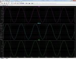
Invertor_6_asc.jpg

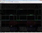
The analysis without the impedance measurement (the RLoad is chosen such that Islanding will occur):
Invertor_6_no_drop_raw.jpg

The analysis with impedance measurement (again, RLoad is chosen such that Islanding would occur):
Invertor_6_with_drop_raw.jpg

The LTSpice files:
View attachment LInvertor_6.zip

The next step would be adding the PWM drive I think, including the decreasing of the current to deliver by the invertor when its source voltage becomes too low.

Please supply your remarks on the current design.

Thanks in advance!
 
Last edited:

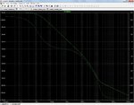
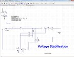
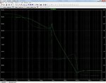
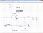
Hi, I tried to do some stability (phase margin) measurements, and the results I get are poor: both in current stabilisation mode (the mode in which the invertor is connected to the grid), as in voltage stabilisation mode (the mode in which the invertor is not connected yet to the grid). At a gain of 0 dB the pahes has already crossed the 180 degrees phase shift.

Most of the problems are related to the way the output filter looks: 1 mH coil in series with the load, with, after that a 40 uF capacitor across the load. Both are there in anticipation of how the power stage (B2 in the current stab mode, B1 in the voltage stah mode) will look: a PWM type circuit.

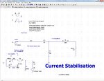
The way of measurement is a classical one: I put an AC source in the minus input line of the op-amp and measure the feedback voltage divided by the op-amp input voltage. Of course I short circuit the original voltage sources while doing the measurement:
In the current stabilisation mode it was originally on the + input of the op-amp, in both the voltage stabilisation mode and the current stab modes the "grid" was across RLoad.

The current stabilisation mode (connected to the grid):
CurrentStab_asc.jpg CurrentStab_Raw.jpg
View attachment Inverter_Stability_Current.zip

The voltage stabiliastion mode (not connected to the grid):
Voltage_Stab_asc.jpg Voltage_Stab_Raw.jpg
View attachment Inverter_Stability_voltage.zip

Who can help me please with this possible stability problem?
Thanks in advance!
 

Status
Not open for further replies.

Part and Inventory Search

Welcome to EDABoard.com

Sponsor

Back
Top