Continue to Site

Welcome to EDAboard.com

Welcome to our site! EDAboard.com is an international Electronics Discussion Forum focused on EDA software, circuits, schematics, books, theory, papers, asic, pld, 8051, DSP, Network, RF, Analog Design, PCB, Service Manuals... and a whole lot more! To participate you need to register. Registration is free. Click here to register now.

Why is an unloaded buffer showing an offset ?

Status
Not open for further replies.

anushaas

Member level 5
Joined
Jan 4, 2011
Messages
84
Helped
0
Reputation
0
Reaction score
0
Trophy points
1,286
Activity points
1,979
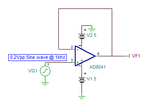
I am using an AD8041 IC as a buffer for a 0.2Vpp sinewave input at 1kHz from the function generator.The circuit is set on an NI Elvis II+ board.The buffer is unloaded but there occurs some offset at the output of the buffer.
Why is this happening?
 

Can you post a schematic?

Looking at the datasheet, you have an input offset voltage of 7 mV max. You also have an input bias current of up to 3.2 microamps (!). These could certainly cause an offset at the output of the buffer!
 

Hi,

"some" offset is no value you will find in a datasheet.
Therfore we can not say if "some" offset is OK or not.

0.2Vpp and 1kHz are values you can calculate with, but unfortunately both don´t relate to the offset problem.

Klaus
 

Can you post a schematic?

Looking at the datasheet, you have an input offset voltage of 7 mV max. You also have an input bias current of up to 3.2 microamps (!). These could certainly cause an offset at the output of the buffer!

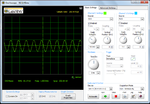
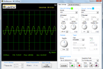
This is the waveform at the input of buffer:
Before buffer.png

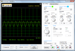
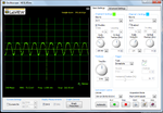
The output of unloaded buffer is as below:
After buffer.png
 

Hi,

your scope pictures are meaningless without schematic.

Klaus
 

Hi,

your scope pictures are meaningless without schematic.

Klaus

Here is the schematic:

Circuit.png

The waveforms shown above are VG1(without offset) and VF1(with offset)
 

Hi,

no resistor involved?

What´s the source resistance of your frequency generator?

What happens when you measure without signal?
What says a DMM measurement?

Klaus
 

AD8041 closed loop gain for G=+1 is heavily peaking, with a bit of capacitive load or without the required supply bypass capacitors placed directly at the amplifier chip, you easily get self oscillations in the 100 MHz range. It could well explain the observed offset.

Suggestion: If you don't have the instruments to measure high frequency signals, don't use 100 MHz OPs.
 

Your schematic has nothing to supply the input bias current to the opamp. If it is the signal generator then its resistance will cause the offset voltage.
Add a same value resistor in series with the (-) input so that the bias currents cancel.
 

The Elvis II function generator has 50 ohms output, so it doesn't cause noticeable offset by it's impedance.

Perhaps we can see a photo that clarifies the complete test setup?
 

Maybe the generator has an AC output impedance of 50 ohms but a DC resistance that is infinity?
Is this project only a simulation??
 

Your schematic has nothing to supply the input bias current to the opamp. If it is the signal generator then its resistance will cause the offset voltage.
Add a same value resistor in series with the (-) input so that the bias currents cancel.

Thank you Sir.That helped.I put a pot in series to negative input,adjusted it till the offset is removed
 

Hi,

it seems the input of your OPAMP was NOT free of DC.
And it seems the scope was not directely connected to the OPAMP input.

--> That´s why I asked about the DMM measurement.

The resistor my be around 50kOhms. This may affect upper cutoff frequency.
Your gain may not be flat anymore. Please check on this.

Klaus
 

The resistor my be around 50kOhms. This may affect upper cutoff frequency.
Your gain may not be flat anymore. Please check on this.
If the amplifier wasn't oscillating before, it surely will now.
 

[Moved]How to remove DC offset from signal?

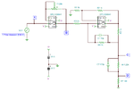
I am implementing the following schematic on a NI ELVIS II+ board
HCS.png

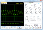
The wave form at point A in the schematic is shown below:
A.png

Initially,without a POT in the feedback path of OP1,the waveform at point B showed an offset as can be seen below:
B without POT.png

Later,a 20k pot was introduced in the feedback path(shown in schematic) and it was adjusted to get the following waveform:
B.png

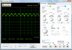
However,the waveforms at points C and D still show some offset as can be seen below:

Waveform at C:
C.png

Waveform at D:
D.png

How can I get rid of this offset?I tried introducing a 1uF capacitor in series before point C.
The waveforms at C and D obtained then were as follows:

Waveform at C:
C with 1uF cap.png

Waveform at D:
D with 1uF cap.png

How can this offset be eliminated?The circuit need to operate at a frequency range of 1Hz to 1MHz.The load shown in the
schematic is the maximum load.
 

The combination of the first C & D (4th and 5th) waveforms makes no sense. Either the oscilloscope has an offset error, or the output offset is changing when you connect the oscilloscope probe. In the latter case, it's most likely a case of high-frequent self oscillations, see my previous post #8. Also the distorted output waveform suggests an oscillation or other serious hardware problem.

My suggestion is to try a user friendly 10 to 20 MHz GBW OP in your circuit.
 

Hi,

the measurement of input (A) and output (B) in configuration without feedback resistor do not fit either.

If the offset is caused by the bias current then you see it also in (A).
The deviation in offset voltage between input and output is max. 7mV per datasheet.
--> maybe the OPAMP is defective, or the measurement is wrong.

****

Is it a breadboard circuit? Do you have a good ground point with star connection?

Do you see strange signals when you change the x-axis timing to us/dev or ns/dev?

****
I don´t understand the second stage. It seems to be a difference amplifier, but then there is the C1/R4 combination feedback to non inverting input.
A feedback to non inverting input is always critical.

Klaus
 

One key assumption is that this particular part is
pristine. After checking that the supplies are what
you think they are, I'd swap out for another part
and see whether the issue persists, or changes.

A little handling ESD can really whack op amp input
attributes.
 

I don´t understand the second stage. It seems to be a difference amplifier, but then there is the C1/R4 combination feedback to non inverting input.
A feedback to non inverting input is always critical.
It's a classical Howland current source circuit. But a singular capacitor in the positive feedback branch without corresponding capacitor in the negative branch reduces the phase margin.
 

Hi,

thanks for the info.

I just goggled about it and reviewed the schematic here.

In some schematics there is a feedback capacitor to the inverting input. This makes sense to stabilise the circuit.

--> But here is one to the non inverting input. @anushaas: please check on this.

**
The high bias current and offset voltage make the OPAMP not suitable for a current source.

Building a current source and feeding the signal to known resistors make - on the first sight - no sense.
I assume this is some kind of measurement circuit, and at least one resistor/impedance is unknown.

Klaus
 

Status
Not open for further replies.

Similar threads

Part and Inventory Search

Welcome to EDABoard.com

Sponsor

Back
Top