Continue to Site

Welcome to EDAboard.com

Welcome to our site! EDAboard.com is an international Electronics Discussion Forum focused on EDA software, circuits, schematics, books, theory, papers, asic, pld, 8051, DSP, Network, RF, Analog Design, PCB, Service Manuals... and a whole lot more! To participate you need to register. Registration is free. Click here to register now.

SolderMask issues with LQFP 100

Status
Not open for further replies.

leolib2004

Junior Member level 3
Joined
Jan 27, 2012
Messages
27
Helped
0
Reputation
0
Reaction score
0
Trophy points
1,281
Activity points
1,556
Hi,

I used Eagle to do my board and now that I finished I sent my gerber files to 4PCB. I used freeDFM but I get these results:

Insufficient SMT Soldermask Clearance (100 violations)

Requirements:We require a minimum of .003" soldermask clearance. This is achieved by a soldermask relief .006" larger than the associated copper pad.

Resolution:While too small a relief can cause your pads to be partially covered by soldermask, too large a clearance can cause traces to be exposed, causing problems during assembly. The best method is to set all your soldermask reliefs .006 in. larger than their associated pad.


It was automatically fixed and I think I understand why it is problem. If it's too big, there may be bridges and if it's too small that may no be able to solder the components.

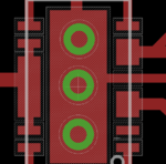
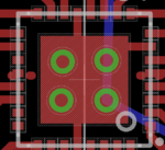
But what can I do if I have a LQFP100 device whose pad's distances are no more than 6 mils... It will be imposible to have clearance there... I also have other components that I created using the default parameters and they have a tiny gap and one does not have a gap at all and I downloaded it from Cadence. Images attached.

I guess I have to trust them but I would like to know if I have another option...

Thank you!

https://obrazki.elektroda.pl/2342436300_1446123496.png
https://obrazki.elektroda.pl/6295045700_1446123496.png
 

Attachments

  • Screen Shot 2015-10-29 at 9.32.32 AM.png
    Screen Shot 2015-10-29 at 9.32.32 AM.png
    43.5 KB · Views: 117
  • Screen Shot 2015-10-29 at 9.32.44 AM.png
    Screen Shot 2015-10-29 at 9.32.44 AM.png
    51.9 KB · Views: 119

Use metric for a start, most modern components are hard metric, look yup IPC-7351 and associated documentation like the universal grid system by Tom Hauser.
In the library do solder mask pads the same size as the standard pad, these can then be adjusted to suit during board fabrication (DO NOT OVERSIZE SOLDER MASK PADS IN THE FOOTPRINT LIBRARY).
What is the pitch of the LQFP100, I have used numerous QFP packages with 0.5mm pitch and l always insist on a dam of solder resist between the pads otherwise there are to many soldering problems.
 

Hi,

EAGLE --> DRC --> MASKS --> STOP (adjust those values).

If you are not sure what values to use, then contact your assembling company. The PCB manufacturer should also give you some hints.

Klaus
 

Do it one to one and change it depending on the complexity of the design... WE control the design not the PCB fabricator, they will want the biggest gap they can get away with or worse block out the whole row of pins.....
 

Hi All,

Thanks for your help. I use metrics but Advanced Circuits doesn't. At least for their freeDFM service.
So, the best thing to do is to have them equally sized as the pads, right?
I have created other manually and the default setup, in Eagle, made them overlap. I can change that. The one I am using for the ATSAM processor has a tiny gap in between but the relation isn't 1-1 with the pads...
I am currently waiting for a response from them. My board will be checked by a "human", as they said.
So "Marce", what's the best for designers in these cases? How can the complexity change this? They mentioned I could do the 1:1 relation but they would have to use LDI to make it which will add some extra cost. Does that make sense to you?
They are algo going to do the assembly, so, if I follow what they say they won't deliver a board full of short circuits. I hope so.
 

Requested 3 mils (75 µm) soldermask clearance is a coarse PCB technology and doesn't well fit designs with 0.5 mm or even lower pin spacing. I usually set 2 mils (50 µm) all round soldermask expansion for standard fine pitch SMD boards and choose a supplier that can provide it.

You might be able to comply with the manufacturers design rules by reducing the pad size. Or increase the respective mask pads to form a single cutout with no separating strips, which brings up a higher risk of solder shorts, unfortunately.
 

Thanks FvM.

What about LDI?
Can you suggest me a supplier from the United States that you have worked with and can handle these requirements?
 

I believe, 2 mils all round solder mask expansion will work for your design and should be managed by most PCB suppliers.
 

That would leave 1.9 mils as the spacing for the pads of the LQFP 100. Does that seem reasonable too?
 

You mean the minimum mask-to-mask feature, the spacing of the soldermask pads? It should be at least 2 mils, possibly more depending on the PCB technology, otherwise there's a risk of small mask strips breaking off and lying around on the pads.
 

Yes, that's what I meant. So, it would be somehow impossible for the LQFP100 as the spacing between pads is just 5.9 mils...
 

Not impossible, just slightly above useful dimensions. I don't think it's absolutely required to have 0.35 mm wide pads? 0.3 or 0.32 would work as well, many 0.5 mm pitch TQFP footprints are suggesting even 0.28 mm width.
 

Hi All,

Thanks for your help. I use metrics but Advanced Circuits doesn't. At least for their freeDFM service.
So, the best thing to do is to have them equally sized as the pads, right?
I have created other manually and the default setup, in Eagle, made them overlap. I can change that. The one I am using for the ATSAM processor has a tiny gap in between but the relation isn't 1-1 with the pads...
I am currently waiting for a response from them. My board will be checked by a "human", as they said.
So "Marce", what's the best for designers in these cases? How can the complexity change this? They mentioned I could do the 1:1 relation but they would have to use LDI to make it which will add some extra cost. Does that make sense to you?
They are algo going to do the assembly, so, if I follow what they say they won't deliver a board full of short circuits. I hope so.

I am on a customers site so don't have access to all my resources. IPC-7351 standard is 1:1 the manufacturer can then increase the soldermask size to suite the board design and their processes, I put a note in my manufacturing instructions saying that they can increase the solder mask clearance provided there is a solder dam between ALL pins....
Having the boards made correctly so they can be soldered fault free is better than getting your ass kicked by assembly because of solder bridges between pins.
 

That's what I am going to do. Have 2 mils on both sides of the pad and have 0.3 mm as width for the pads. I downloaded a different library and that's what they do. That's seem fine for Advanced Circuits too. Thanks.

- - - Updated - - -

Marce, that's seems reasonable too. I asked this to Advanced Circuits and they seemed to prefer the option I mentioned before. Maybe, the next time I will follow your path. It seems easier on my side. I need to get this asap so I will hear what they said. Thanks for your help too!
 

Hi guys,

Regarding this same package, LQFP 100. I have found differences with the suggested land patterns in the pad's length. I found some places that it is 1.35 mm but in others it is 1.50 mm (as QFP or TQFP 100) (http://www.atmel.com/images/atmel-8...es-surface-mount-packages-applicationnote.pdf)

What is the best to do here or according to the standard? Will it be ok if it's of 1.35mm. I currently have it of 1.35mm and I am not sure if it worth to make it a little bigger.

Thanks.
 
Last edited:

Status
Not open for further replies.

Part and Inventory Search

Welcome to EDABoard.com

Sponsor

Back
Top