tony_lth
Advanced Member level 5
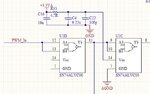
When I debug one design of 2-Input Positive-Nand-Gate, I found it was very hot sometimes and oscilated, but when I power-off it for several minutes, then it works well again.
What is the issue?
1. Should I put some resistors as load for each output?
2. Or it should not be connected as such way?
Thanks.
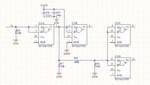
What is the issue?
1. Should I put some resistors as load for each output?
2. Or it should not be connected as such way?
Thanks.