Continue to Site

Welcome to EDAboard.com

Welcome to our site! EDAboard.com is an international Electronics Discussion Forum focused on EDA software, circuits, schematics, books, theory, papers, asic, pld, 8051, DSP, Network, RF, Analog Design, PCB, Service Manuals... and a whole lot more! To participate you need to register. Registration is free. Click here to register now.

Opamp with ICMR min upto 0.6V

Status
Not open for further replies.

predator89

Member level 1
Joined
Sep 7, 2015
Messages
37
Helped
0
Reputation
0
Reaction score
0
Trophy points
1,286
Location
Denmark
Activity points
1,610
I want to design a opamp with ICMR range 0.6V to 2.7V for VDD=3.3V and VSS = gnd

But as ICMR min = VSS - VGSsat(M5) - Vt(M1)
I am able to get ICMR min upto 1.4 V. Is there any other topology or method to reduce ICMR min further.

opamp.jpg
 

Use M5 to operate in subthreshold region (VGSsat(M5) < 200mV), or - if this is not sufficient - use an NMOS/PMOS parallel .
 
Thanks. I'll try this approach.

- - - Updated - - -

Thanks. I'll try this approach. Do you have any source for the design procedure.
 

- - - Updated - - -
I'll try this approach. Do you have any source for the design procedure.
Which one? Subthreshold region operation for M5 (simple method) or NMOS/PMOS parallel rail-to-rail input architecture (more complex)? The paper which I linked above shows the latter method.

And don't forget to reveal your process size and your previous schematic, incl. W/L sizes.
 

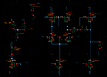
I want to try "Subthreshold region operation for M5 (simple method)". I have attached the screenshot of my design where i achevied min ICMR of 1V but i need to get it to 0.6V. My design is based on 180nm technology and VDD is 3.3V.
2satgeopamp2.png
2stageopamp.png

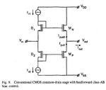
Also from the paper suggested by you I found the the class ab output stage(image atached), which i am planning to implement for my design with output voltage range of 0 to 40V. Where i would be using HVMOS. So is it possible with this architecture?

Class AB SF2.png
 

you can increase VDD, but need to insure the potentiel between D and S of each mos < VDD
 

Which one? Subthreshold region operation for M5 (simple method) or NMOS/PMOS parallel rail-to-rail input architecture (more complex)? The paper which I linked above shows the latter method.

And don't forget to reveal your process size and your previous schematic, incl. W/L sizes.

I have attached the images in my comment which shows the W/L vlaues
 

I want to try "Subthreshold region operation for M5 (simple method)". I have attached the screenshot of my design where i achevied min ICMR of 1V but i need to get it to 0.6V. My design is based on 180nm technology and VDD is 3.3V.

Seems you have NMOSFETs with a very low threshold voltage available: V(V3) - Vs(M12,M13) = 0.2V . So try and reduce the Vds of M12 & M13 by operating them in moderate or weak inversion (subthreshold) region - by creating an extra Vbias for them: strongly increase their W/L ratio; I think you could use min. L for this purpose.

Also from the paper suggested by you I found the the class ab output stage(image atached), which i am planning to implement for my design with output voltage range of 0 to 40V. Where i would be using HVMOS. So is it possible with this architecture?

Yes, I think this should be possible if you can renounce on two diode voltages and two drain-source saturation voltages of the output range (s. explanation of Fig. 9). I guess this should be allowable for a 40V output supply. Otherwise you need a (much) more complex output architecture (s. the rest of the paper).
 
Yes, I think this should be possible if you can renounce on two diode voltages and two drain-source saturation voltages

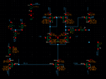
I tried this class ab output stage today. But i am having a clipped output.

Output without FB.png

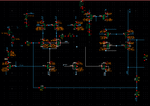
I tried giving a negative feedback, but the problem i am facing problem with keeping the input bias voltage to 2V. due to which the + and - input nmos are not baised at same voltage and the bias of the further stages goes wrong. Could you suggest me with the feedback topolgy

opamp with feedback.png
 

I tried this class ab output stage today. But i am having a clipped output.
Of course: R9 + R8 are in parallel to R11 (V3 has an output impedance of 0Ω), so your adjusted gain is around 100 , not 10 as you probably intended.

I tried giving a negative feedback, but the problem i am facing problem with keeping the input bias voltage to 2V. due to which the + and - input nmos are not baised at same voltage and the bias of the further stages goes wrong. Could you suggest me with the feedback topolgy

I can see that the input voltage is 2V at both inputs, and bias at the following stages doesn't seem to be so wrong.

Remove V3 (and perhaps replace R8 and R9 by wires, they aren't necessary), so you achieve a gain of 10 for ac and also for DC, which should result in about 1/11 of the required quiescent output voltage of 20V (half supply voltage), i.e. about the required 2V at the input - adjust R11 to achieve the necessary half supply voltage of 20V at the output. Let V2 be connected between VIN and VIP.
 

Remove V3 (and perhaps replace R8 and R9 by wires, they aren't necessary),

Then what would be the calculation for gain. As for negative feedback the gain is Rf/Rin, but if i replace by wire how wud be the gain calculation.
 

Then what would be the calculation for gain. As for negative feedback the gain is Rf/Rin, but if i replace by wire how wud be the gain calculation.

What I suggested was for the test bench; for application you need a different setup, depending on using your opamp as an inverting or a non-inverting amplifier. If you use it in non-inverting mode (input to VIP), its gain would be 1+(R10/R11). Of course you have to provide the correct DC bias to VIP also - same as in the inverting mode case.
 

What I suggested was for the test bench; for application you need a different setup, depending on using your opamp as an inverting or a non-inverting amplifier. If you use it in non-inverting mode (input to VIP), its gain would be 1+(R10/R11). Of course you have to provide the correct DC bias to VIP also - same as in the inverting mode case.

I tried giving the feedback by keeping the bias same at VIN and VIP of 2V, I managed to get the gain of 10X
1_1.png
1_2.png

But when i changed the resistor values to obtain gain of 18X which is my required gain, I am getting a weird output.
2_1.png
2_2.png

Please suggest how would i get gain of 18X by using the feedback
 

But when i changed the resistor values to obtain gain of 18X which is my required gain, I am getting a weird output.
Please suggest how would i get gain of 18X by using the feedback

With your feedback network the DC gain is (R10+R11+R12+R5)/R5 = 19 (simple voltage divider calculation), so an input voltage of 2V fits well with the output voltage of 38V of the initial DC solution; the ac gain is -(R10+R11+R12)/R5 = -18 as you intend. Even if Vout1=1.914V seems to be fine for the output of the 1st part of the opAmp, it's probably too high for the input of the 2nd opAmp part and sends VOUT to GND potential.

To overcome this problem I think you'd have to separate the DC and ac feedBack paths, which unfortunately needs 1 or 2 additional caps. You'd have to feed the DC gain = 22.5/2 = 11.25 to VIN, and also the required ac gain = 18 to VIN, by splitting the series resistor R5 into 2 parts and bridging one of them by a cap which makes it ineffective for ac - so you adjust for the higher ac gain. This RC combination generates the upper limit of the unwanted ac feedback, or the lower limit of your ac bandpass. Supply VIP's DC voltage as before, or supply VIN's DC to VIP via one more RC combination, by this killing the ac part of the feedback at the VIP input - one more RC combination responsible for the lower limit of your bandpass.
 
Status
Not open for further replies.

Similar threads

Part and Inventory Search

Welcome to EDABoard.com

Sponsor

Back
Top