Continue to Site

Welcome to EDAboard.com

Welcome to our site! EDAboard.com is an international Electronics Discussion Forum focused on EDA software, circuits, schematics, books, theory, papers, asic, pld, 8051, DSP, Network, RF, Analog Design, PCB, Service Manuals... and a whole lot more! To participate you need to register. Registration is free. Click here to register now.

Inverted Parabola problem in BGR

Status
Not open for further replies.

DJP1992

Newbie level 5
Joined
May 31, 2012
Messages
8
Helped
0
Reputation
0
Reaction score
0
Trophy points
1,281
Location
INDIA
Activity points
1,361
low_bgr.jpg
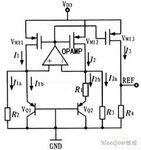
Hi ,everyone i am trying to design a low voltage BGR.I am using 90nm Technology with 1v supply and vref is 700mV.Eventhough,I am getting variation of around 8mV across corners(SS,NN,SF,FS,FF) but vref curve is inverted parabola(i.e. U)(vref v/s temp).I am not able to figure out what may be the possible reason.Can anyone help me out.
Obtained output:
Phase margin=72 deg
PSRR=-38dB

IS the output acceptable or is it compulsory that we must get normal parabola(inverted U) curve.
 

This is caller "curvature" and has been one of the main
challenges since the first bipolar bandgap designs. Many
papers on curvature correction out there, and many of
them are blind alleys you don't want to go down (for
example, the idea that you should "correct" the 2nd
order error with a cubic term tends to bring more pain
than relief).

The parabolic character sets a minimum deflection
over temp which limits your ability to trim to a low
across-envelope max error.

Base current and Rb is one error source. So is the
higher order tempco (2nd, 3rd, ...) of resistors. A
dead flat metallic resistor does not suffice to eliminate
it all, but at least gets rid of the resistor contribution
(if you can have it - used to be a common feature
of older precision analog processes, but seldom seen
in digital or "mixed signal" (i.e. digital plus MIM cap)
foundry flows.

I suspect plenty of process engineering at ADI and
Linear Tech for the resistors of the special flows their
high precision continuous-time reference products run
on. We were never able to come close to their art
using more generic linear processes, even ones with
thin film metallic resistors.

Another approach involves a digital cal-map, a temp
sensor, a crude ADC and a trim-DAC pushing a
compensating current into the bandgap core, or
a voltage summed with its output. In higher density
nodes this can be more area-economical than an
E-trim (fuse, laser) block. It can take you to a dead
flat tempco at the output.
 
  • Like
Reactions: erikl

    erikl

    Points: 2
    Helpful Answer Positive Rating
View attachment 122176
I am getting variation of around 8mV across corners(SS,NN,SF,FS,FF) but vref curve is inverted parabola(i.e. U)(vref v/s temp).I am not able to figure out what may be the possible reason.
As dick_freebird pointed out, probably the resistors' TCs (1st and 2nd order, even if they are the same for all resistors!) are mainly responsible for this - you can try it out by using ideal resistors from analogLib.

If so, you can make it a little better by putting together the resistors appropriately from those with pos. and neg. 1st order TCs - if such are available in your process, and are modeled correspondingly.

A further reason would be "not enough perfect", i.e. too asymmetrical layout - but I guess your result is still from preLayout.


Is the output acceptable or is it compulsory that we must get normal parabola(inverted U) curve.
Admittedly a 1% deviation over corners is quite a lot compared to similar BGRs, but the chip-to-chip deviation can be even stronger, see e.g. this paper: View attachment BGR_Performance_CMOS_130nm.pdf

A "normal" parabola curve is not at all compulsory - the only criterion for the max. acceptable deviation is your application requirement.
 

Status
Not open for further replies.

Part and Inventory Search

Welcome to EDABoard.com

Sponsor

Back
Top