Continue to Site

Welcome to EDAboard.com

Welcome to our site! EDAboard.com is an international Electronics Discussion Forum focused on EDA software, circuits, schematics, books, theory, papers, asic, pld, 8051, DSP, Network, RF, Analog Design, PCB, Service Manuals... and a whole lot more! To participate you need to register. Registration is free. Click here to register now.

Is my High-side MOSFET Really Off?

Status
Not open for further replies.

SparkingDog

Newbie level 6
Joined
Feb 12, 2014
Messages
14
Helped
0
Reputation
0
Reaction score
0
Trophy points
1
Activity points
165
I am designing a real high-side switch circuit but my questions really apply to mosfets in general.

The datasheets for discrete mosfets generally specify a Vgs Theshold (example: -0.45V @ Ids=250uA) and an Off leakage current (example: Ids<1uA @ Vgs=0V). In my circuit it is not practical to get Vgs=0; and 250uA is too large a current for my off state.

Question #1: Is there an equation or rule of thumb that allows me to put a bound on Ids for 0<Vgs<Vth ? i.e. sub-threshold Ids (For example: Ids<1uA)

Also graphs of leakage current versus temperature indicate leakage currents which are orders of magnitude smaller than the worst case listed in the spec table.

Question #2: Is the real leakage current the 1uA max in the spec table or the 20nA in the graph?
 

Question #1: Is there an equation or rule of thumb that allows me to put a bound on Ids for 0<Vgs<Vth ? i.e. sub-threshold Ids (For example: Ids<1uA)
Ids rises approx. exponentially with Vgs between Vgs=0 and Vth, so if you know two Ids values in this range, you can draw a curve. But this only makes sense for a single device. And think of Ids' temperature dependency!

Also graphs of leakage current versus temperature indicate leakage currents which are orders of magnitude smaller than the worst case listed in the spec table.

Question #2: Is the real leakage current the 1uA max in the spec table or the 20nA in the graph?
Such graphs usually show typical values, whereas specs give max. values (hopefully at a specified max. temperature), which perhaps are tested for non-exceedance - if you are lucky.

So for a single device you could get along with the a.m. method (max. temperature considered!), but think of a possible necessity for replacement!

You never could risk this for volume production. In the latter case you should have an auxiliary (higher) voltage which allows you to apply Vgs=0 or even Vgs > 0 (PMOS).
 

Such graphs usually show typical values, whereas specs give max. values (hopefully at a specified max. temperature), which perhaps are tested for non-exceedance - if you are lucky.

I realize that the graphs are for typical values. I was just surprised by the orders of magnitude difference. Also I was once told by an App Engineer (about a microcontroller) that the 1uA leakage current spec in their data sheet was just a convenient tested limit and not the actual expected max leakage which was much less. So I thought this might be a similar scenario. It seems that nearly every IC and device I look at has a 1uA max leakage spec!

You never could risk this for volume production. In the latter case you should have an auxiliary (higher) voltage which allows you to apply Vgs=0 or even Vgs > 0 (PMOS).

Applying a gate voltage which is higher than the source is not very practical for a FET which is being used to switch off the power. It is my belief that this type of circuit is used all the time and thus probably always works as expected. Most likely because Ids drops off so quickly below Vth (exponentially, as you said.). But if I am going to minimize battery drain; it would be useful to be able to place some sort of boundary on sub-threshold Ids.

Note: Temperature is not much of an issue because once the FET is mostly off, it will cool to room temp.
 
Last edited:

Why can't you put Vgs to 0V?
Post your circuit diagram.

The question is about FETs in general - not my circuit. But the problem is that, generally, if you are building low power circuits from discrete FETs you must use high value resistors as pull-ups/pull-downs. Ids leakage of even 1uA creates significant voltages across those resistors. 1uA*100K=0.1V. While 0.1V is below the threshold; it is not 0V. So how much leakage current will there be at 0.1V?

While I could make this Vgs voltage arbitrarily small by using lower value resistors or by adding more FETs (complexity); both of these approaches increase power consumption and/or cost. In any case, using real parts with non-zero resistances and non-zero leakage currents, the Vgs of a high-side switching FET will never be zero - unless you add an even higher voltage supply which is often not practical.

It would be much better if there was some way to know that Vgs=0.1V was good enough. And, intuitively, I feel that there must be.
I also suspect the the stated maximum leakage current is much higher than what will be seen in real devices.

And I think that it is the combination of lower than stated leakage and exponential drop off of Ids below threshold which allows most circuit designers to get by without considering this issue. But I would like to have more than intuition to justify my design choices.

- - - Updated - - -

I know nothing about semiconductor physics, but I have found several references that state that Ids drops by a factor of 10x for every n*60mV drop in Vgs; where "n" is a characteristic of the FET device (1 < n < ?).
n= 1+ Cb/Cg; where Cb is bulk capacitance, Cg is gate capacitance.

https://en.wikipedia.org/wiki/Subthreshold_slope

This is exactly the kind of "rule" I was looking for. If I only knew what the range of "n" was for real devices. Or how to estimate "n" from the data sheet specs.
 

If you use a CMOS circuit to drive the MOSFET gate then you can drive the Vgs to between 0V and the supply voltage with no power dissipated, other than the leakage current of the CMOS circuit and the MOSFET.
You can't really do better than that.
 

If you use a CMOS circuit to drive the MOSFET gate then you can drive the Vgs to between 0V and the supply voltage with no power dissipated, other than the leakage current of the CMOS circuit and the MOSFET.
You can't really do better than that.

Again, my question is about the properties of FETs not about a solution to a specific circuit.

But responding to your suggestion:
A CMOS IC running off battery voltage to control the P FET could not be connected to logic powered from the regulated supply without level translation - probably a FET with a pull-up resistor - which is what the CMOS IC is replacing. Also static supply current for CMOS ICs is often spec'ed with the inputs shorted to the rails; it can rise significantly as the inputs deviate from the rails - which just shifts the problem. (But, probably some conveniently spec'ed device could be found.)

Adding a CMOS IC that can run directly off battery voltage adds a $0.10-$0.20 part, a new line item to the bom, uses PCB real estate, and adds $0.10 - $0.20 in assembly costs. Having an equation or rule for the FET cut off costs nothing.
 

Equations can be found in analog design text books. But I don't believe that it makes sense to refer to equations in this case, equations can only represent the typical values, the behavior of an average transistor. A design must consider type variations. You better refer to min/max values in datasheets.
 

I have found several references that state that Ids drops by a factor of 10x for every n*60mV drop in Vgs; where "n" is a characteristic of the FET device (1 < n < ?).
n= 1+ Cb/Cg; where Cb is bulk capacitance, Cg is gate capacitance.

https://en.wikipedia.org/wiki/Subthreshold_slope

This is exactly the kind of "rule" I was looking for. If I only knew what the range of "n" was for real devices.

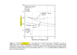
Here's the right value for the subthreshold factor n from Binkley's book: View attachment subthreshold-factor.pdf
 

Equations can be found in analog design text books. But I don't believe that it makes sense to refer to equations in this case, equations can only represent the typical values, the behavior of an average transistor. A design must consider type variations. You better refer to min/max values in datasheets.

You might be right; but, in the absence of specific authoritative information to the contrary I will continue to hope for a solution.
These are my reasons:
1. Much of the process variation is accounted for by the Vth spec. It is a worst case that is tested in production. It provides a worst case, specific data point on the Vgs/Ids curve which is adjacent to the area of interest.

2. I am not looking for a precise prediction of sub-threshold Ids, but only an upper bound on Ids that can be used to determine a "good enough" result. Given the exponential character of the Ids curve, the rule/equation could have orders of magnitude of safety factor and still be useful.

3. I think I may have found the equation/rule. I would be comfortable using a subthreshold slope of n*60mV/decade if I could get authoritative confirmation that n<1.5 for any practical FET.
Example using max leakage spec as a point on the curve:
Using data from my specific part (Ids=250uA @ Vgs=0.45V ) and (Ids<1uA @ Vgs=0) as two points on the curve yields a slope of 188mv/decade (n=3.1). I think the real value of "n" is much lower.

4. (I hate being pedantic but) Virtually all low power designs have to make some assumption about Ids with |Vgs|>0. I am just looking for a little more precision with the hope of getting a better design.
 

Here's the right value for the subthreshold factor n from Binkley's book: View attachment 122181

Thanks that is just the kind of authoritative source I was looking for. Unfortunately the highlighted section in the link only gives an example value for "n". What is needed is a maximum practical value for "n". At the bottom of the linked page the author mentions a minimum value for "n"; does he continue on the next page to discuss a maximum?

- - - Updated - - -

So for a single device you could get along with the a.m. method (max. temperature considered!), but think of a possible necessity for replacement!

What is the "a.m. method"?
 

Thanks that is just the kind of authoritative source I was looking for. Unfortunately the highlighted section in the link only gives an example value for "n". What is needed is a maximum practical value for "n". At the bottom of the linked page the author mentions a minimum value for "n"; does he continue on the next page to discuss a maximum?

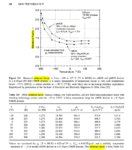
You can find a lot of values for the substrate- or subthreshold-factor in literature, but I think n=1.5 is a good worst case value for its maximum - which you should use, s. below. The first 2 snippets are also from the Binkley book:

Substrate-factor_vs_inversion.png Substrate-factor_vs_temperature.png View attachment Substrate-factor.pdf

a.m. = above mentioned
 
That is very helpful. I think I will use 100mV/decade for design and just keep an eye out for any risks or contrary results.

I also suspect that typical max leakage specs may be overly pessimistic (it's suspicious that it is so often 1uA) - any insight about that?

For example using my specific device Vth (Vgs=-0.45 @ Ids=250uA) the max Ids @ Vgs=0 found using the subthreshold slope method would be: 0.45V/0.1V = 4.5; Ids < 250uA / 10^4.5 = 8nA

So does some non-channel path or effect dominate at Vgs=0 making the max leakage two orders of magnitude higher than predicted by the slope method?

Or is it as I suspect that the Vgs=0 leakage spec is just an arbitrarily chosen "good enough" spec for production test?

I understand that many people would just say accept what the datasheet says and design around it; but, when pushing on the cost/performance limit I feel the need to really understand what's happening in the gaps. And numerous times I have found errors and inconsistencies in the datasheets.
 

I also suspect that typical max leakage specs may be overly pessimistic (it's suspicious that it is so often 1uA) - any insight about that?
Or is it as I suspect that the Vgs=0 leakage spec is just an arbitrarily chosen "good enough" spec for production test?
This is quite possible. May be it's set so high that they just have to run random sampling tests.

For example using my specific device Vth (Vgs=-0.45 @ Ids=250uA) the max Ids @ Vgs=0 found using the subthreshold slope method would be: 0.45V/0.1V = 4.5; Ids < 250uA / 10^4.5 = 8nA
So does some non-channel path or effect dominate at Vgs=0 making the max leakage two orders of magnitude higher than predicted by the slope method?
At MOS transistors the always existent bulk-to-drain reverse-biased junction diode usually has maximal the same leakage current as the transistor @ Vgs=0 - rather less - it depends on Vds and on temperature, too, of course. Should also be specified, anyway. Ids measurements always include this current.

If you have to go down into the nA range, you'd also have to look out for residues of foil, foam, or cleaning agents at the transistor and the PCB.

I understand that many people would just say accept what the datasheet says and design around it; but, when pushing on the cost/performance limit I feel the need to really understand what's happening in the gaps. And numerous times I have found errors and inconsistencies in the datasheets.
For volume production you should always respect the border values, as FvM pointed out above - otherwise you dismiss the manufacturer of their responsibility.

What else? You could run your own volume tests at your application conditions.
 

Status
Not open for further replies.

Similar threads

Part and Inventory Search

Welcome to EDABoard.com

Sponsor

Back
Top