Continue to Site

Welcome to EDAboard.com

Welcome to our site! EDAboard.com is an international Electronics Discussion Forum focused on EDA software, circuits, schematics, books, theory, papers, asic, pld, 8051, DSP, Network, RF, Analog Design, PCB, Service Manuals... and a whole lot more! To participate you need to register. Registration is free. Click here to register now.

Connecting PCB trace to output of LC filter

Status
Not open for further replies.

matt11

Newbie level 4
Joined
Jun 22, 2012
Messages
7
Helped
0
Reputation
0
Reaction score
0
Trophy points
1,281
Activity points
1,362
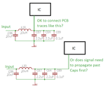
When multiple output capacitors are used in an LC filter does it matter where the PCB trace connects to the output of the filter?
Would it matter if the PCB trace was connected between two of the output capacitors or should it be connected at the last capacitor in the chain? (See attached Figure)
I realize that ideally it would not matter, I'm just wondering if the signal needs to actually propagate past all filter components before being applied to additional parts of the design?
 

Attachments

  • Figure.png
    Figure.png
    18.7 KB · Views: 75

Depends on current rise time, it wont matter for most low power designs electrolytics. but for 0.1uF ceramics, the purpose is for lower ESR and lower ESL.

If IC needs one close as per design guide, then it must be close to chip.

If you know the track impedance and ripple current, you can compute the voltage drop on your ground tracks or ground plane.
 
Last edited:

Hi,

You show a schematic. The schematic should be drawn for good readability and to visualize the function of the circuit. There is no need to connect it at a special capacitor in schematic. It is a pure layout question.
But for sure it is a method to visualize the problem (like force and sense connections on a shunt resistor)

****
To your question:
In many cases it is not imortant. It is more critical if the power distribution is made with wires instead of a copper plane.
For very critical applications i'd prefer your second solution.

But in detail i'd decide what the goal of the capacitors is.
For example... if you know there is HF ripple coming from the power supply it is a good technique to connect a low capacitance ceramics capacitor next to the power supply entry.

For application when you have analog and digital sections supplied from the same power source...Then you may split the analog and digital section at the bulk electrolytic capacitor and use independent ceramics capacitors at the analog section and the digital section.

But, as said, in most cases the second circuit is a good practice.

Klaus
 

The method which you have shown will be useful for deriving two or more supply and ground lines lines from the single supply and ground lines mainly used for ADC power supply filter circuit. This works better when you place the components very close to the device.

The first method also can be followed if you are going to connect another device or line also at the C89. If not then follow the second method which you have shown.
 

From work I have done for high EMC immunity and from what I have been taught by several SMPS application engineers and a couple of RF engineers on interesting EMC problems, join at the last cap, do not put it half way down a row of capacitors. I have learnt that every last detail is important especially when you need to get EMC up to 18GHz.
I go even more extreme when laying filters out and run the trace directly through the cap pins as this illustration from a document that was done for a project I worked on shows... This is applicable to filter caps as well. I do consider these details critical for PCB design these days for EMC, signal integrity and just general noise control.
Don't forget you can create AC potential dividers using caps, t-ing off before the last cap is effectively doing that...
 

Attachments

  • filter-caps.png
    filter-caps.png
    85.2 KB · Views: 79
  • Like
Reactions: KlausST

    KlausST

    Points: 2
    Helpful Answer Positive Rating
PCB trace length has some inductance, so it can matter for "fast" signals. However, here with 10µH base inductance in the low pass, I wonder if some extra nH from PCB trace length make a difference.

Cap placement: The cap closest to the IC should be the one with the smallest value.
 

In this instance yes, if a Pi filter though, then balance the pi filter.
 

Status
Not open for further replies.

Part and Inventory Search

Welcome to EDABoard.com

Sponsor

Back
Top