Continue to Site

Welcome to EDAboard.com

Welcome to our site! EDAboard.com is an international Electronics Discussion Forum focused on EDA software, circuits, schematics, books, theory, papers, asic, pld, 8051, DSP, Network, RF, Analog Design, PCB, Service Manuals... and a whole lot more! To participate you need to register. Registration is free. Click here to register now.

Would a weak ground plane polygon affect my circuit?

Status
Not open for further replies.

krishnakumar.r93

Member level 2
Joined
Jan 28, 2015
Messages
48
Helped
1
Reputation
2
Reaction score
1
Trophy points
8
Activity points
388
Hi all,

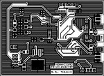
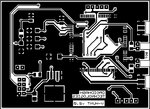
I use Proteus ARES for my PCB designs. When i use a polygon for a ground plane and export the layer as pdf, i get lot of vertical lines in the polygon area instead of solid fill. When i zoom in/out, the vertical lines disappear and i get a solid fill. But when i outsource in to my manufacturer for fabrication, i still get the vertical lines on my board instead of solid fill. There is connectivity, but i feel the plane is weak. Will this vertical lines weaken the ground plane of my circuit?

I have attached the model images of the problem i have. Somebody help me out ASAP.
 

Attachments

  • ground plane - hatched.jpg
    ground plane - hatched.jpg
    328.2 KB · Views: 139
  • ground plane - solid.jpg
    ground plane - solid.jpg
    120.3 KB · Views: 87

Hi,

maybe a wrong setup. the lines should rather overlap than leaving gaps.

This gives no good gorundplane.

Klaus
 

The slots, which is what they look like, will result in all kinds of problems with ground loops running all over the board. This isn't a ground plane.
 

That is a copper pour not a ground plane.
How are you sending data to your manufacturer?
What are the settings for the polygon fill?
 

It wouold suggest to me that too thin a copper code is being used, the d'code in the gerber need IMO to be thicker.
 

The slots, which is what they look like, will result in all kinds of problems with ground loops running all over the board. This isn't a ground plane.

Is the procedure of taking ground connection from the polygon fill wrong..?

- - - Updated - - -

That is a copper pour not a ground plane.
How are you sending data to your manufacturer?
What are the settings for the polygon fill?

I use the copper pour as ground.
I outsource data to the manufacturer as PDF and gerber as well.

- - - Updated - - -

It wouold suggest to me that too thin a copper code is being used, the d'code in the gerber need IMO to be thicker.

@Mattylad: Should i change it in any of my procedure or will it have to be done by the manufacturer.?
 

Hi,

I personally don´t rely on a PDF as data format for PCB manufacturing.

***
Gerber is much better.

Is the procedure of taking ground connection from the polygon fill wrong..?
I don´t know if the procedure is wrong. But the result seems to be wrong.
A true power plane is better than a copper pour. But a good considered copper pour may be almost as good as a true power plane.
(In former there were true "power layers". usually without traces. The data format was negative, with every flash/line generating isolation instead of conductive copper wires. This reduced the amount of data extremely. Nowadays nobody cares about some megabytes of data)

To test: Generate gerber data and use GCprevue (or similar gerber viewer software) to validate the data. If you see gaps, then you should adjust your PCB layout software.
If you don´t see any gaps, then it´s a problem of the PCB manufacturer.

****

I recommend to give valid data to the manufacturer. In my eyes it´s on the designer to generate valid data. My manufacturer is adviced not to change my data, instead he should tell me what to change.
So i´m sure my data are up to date, and if i decide to change the manufacturer I expect no problems.

Klaus
 

I personally don´t rely on a PDF as data format for PCB manufacturing.
I send PDF along with Gerber files.

A true power plane is better than a copper pour. But a good considered copper pour may be almost as good as a true power plane.
I use the polygon as a ground power plane.
polygon fill settings.jpg
 

As it appears that you cannot output this with a thicker line then it appears that it is just a failing of the output process.

What output are you making? rs274 or rs274-x ?
 

So it should not be a misinterpretation of the apetures used.

I remember seeing copper like this when EasyPC did it, boards still came back OK - the manufacturer just filled the whole copper area.
Check with them.
 
Status
Not open for further replies.

Part and Inventory Search

Welcome to EDABoard.com

Sponsor

Back
Top