Continue to Site

Welcome to EDAboard.com

Welcome to our site! EDAboard.com is an international Electronics Discussion Forum focused on EDA software, circuits, schematics, books, theory, papers, asic, pld, 8051, DSP, Network, RF, Analog Design, PCB, Service Manuals... and a whole lot more! To participate you need to register. Registration is free. Click here to register now.

A question about BJT Astable Multivibrators

Status
Not open for further replies.

samy555

Full Member level 4
Joined
May 11, 2010
Messages
207
Helped
0
Reputation
0
Reaction score
0
Trophy points
1,296
Location
Palestine
Activity points
2,963
Hello
From:
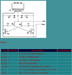
https://www.learnabout-electronics.org/Oscillators/osc41.php

astable-basic[1].gif

I read under Title " Astable Operation ":

01.jpg
02.jpg

I could not understand what is underlined. I understand how each transistor turns on but I could not understand how it becomes OFF
Thanks to everyone who tries to help
 
Last edited by a moderator:

When TR2 starts to conduct, Out2 falls from +9V to (nearly) 0V. This -9V edge is transferred via C2 to the base of TR1, which initially was at 0.6V, and so falls to -8.4V (actually limited by the reverse breakdown voltage of Tr1's emitter-base junction), large enough to shut down Tr1's collector current.
 

When TR2 starts to conduct, Out2 falls from +9V to (nearly) 0V. This -9V edge is transferred via C2 to the base of TR1, which initially was at 0.6V, and so falls to -8.4V (actually limited by the reverse breakdown voltage of Tr1's emitter-base junction), large enough to shut down Tr1's collector current.

ًWhere did -9 volt come from?
 

Thanks to everyone who tries to help

WHen TR1 switches ON from 9V to 0.5V it pushes TR2 Vbe below ground to -8.5V because Vcap does not change instantly.

Unfortunately most transistors are not like diodes and this exceeds the Veb breakdown of -6V typical, so it violates prudent design.
Thus it is better to run from 5V or insert small signal diode in series with base to protect from reverse leakage avalanche failure. (Often original way is found in Chinese toys. ) The-6V absolute MAX has additional margin before actual failure. and depends on temp.and vendor margin.

Better design uses CMOS SChmitt trigger with R feedback and C on input to ground.
 

ًWhere did -9 volt come from?

From TR2's switch-on collector potential change from +9v to 0V transferred by C2 to TR1's base potential change from +0.6V to -8.4V.

The -9V difference means the potential difference between the state after the switching minus the state before the switching - on the oscilloscope seen as a -9V falling edge in time direction.
 

The transistors are actually damaged by the excessive negative voltage produced by that horrible circuit because the emitter-base junction is not designed to withstand avalanche breakdown over and over.
There is a 12V DC to 120VAC inverter on the web that uses this horrible circuit. I fixed it by adding two diodes and two resistors like this:
 

Attachments

  • bad inverter1.PNG
    bad inverter1.PNG
    23.2 KB · Views: 108

@audioguru. I'm not so sure how the your R-CR suppresses -ve Vbe

I indicated the better way was to add CR in series with base as signal diode has larger Vr and lower leakage.

multivib.jpg

SIM link needs java approval < improved version.

This version also has improved rise time using a series R with diode(CR) in each Vbe due to loading effects on Vce. As long as hFE is fairly matched in each, duty cycle is 50%.

Note: Rb is 10x Rc
 

Sorry, I posted the original horrible inverter circuit by mistake. My fixed circuit used diodes like in your circuit but it also had base-emitter turn-off resistors:
 

Attachments

  • bad inverter corrected.PNG
    bad inverter corrected.PNG
    6.3 KB · Views: 99

SIM link needs java approval < improved version.

Hi Tony,

really nice presentation!

But why does the Vbe voltage (left) show a max. voltage of +7.4V (actually not possible) ? May be this is the potential between the diode and the 1k resistor?
 

Yes you are correct.

Notice when mouse pointer is over waveform that the corresponding wire or component colour changes and visa versa.

You can add any waveform by selecting single wire or component, then right mouse add View In Scope

Then on new waveform , right mouse and change view ( painfully only one option at a time)
to Show Peak Value,
(repeat) Show Negative Peak,
... Disable current or voltage,
(repeat) show frequency,
stack or unstack waveform to left..etc

then Menu> File> Export Link

You can also right mouse copy components or group of parts, then ^V to paste, add wires for test points, then view in scope.etc etc. then save into your notepad by Export Text (script) or Export Link

Or start from scratch with
menu> Circuits>transistors>Multivibrators>Astable (enter)

Notice the 1K diode series limits base current, steps output collector voltage instead of slewing RC slowly and R divider ensure threshold still commutates transistors with >0.65Vbe.

hFE is fixed for each transistor and you can change from 100 to 10 on both but not one.

Right click on any component to change property.. even wires to show instant DC Voltage or current.

Scope always shows peak values on entire wave.

In the end this multivibrator sucks a lot of current, but the collector R could be a useful external load.

You can add any component or very simple IC (Op Amp) but some characteristics are estimated like Diode Vf @1A, others are ideal like current out of Op Amp and bandwidth, so to make realistic, one must add parasitic or intrinsic resistance, capacitance, inductance for more accurate simulation. ( requires knowing the limitations but quick and dirty way to show proof of concept)

I like the presentation style better than Vspice.
 
  • Like
Reactions: erikl

    erikl

    Points: 2
    Helpful Answer Positive Rating
Thanks to SunnySkyguy erikl and Audioguru

Sorry, I posted the original horrible inverter circuit by mistake. My fixed circuit used diodes like in your circuit but it also had base-emitter turn-off resistors:
broken link removed
I need to ask about the importance of D1 D2 R1 and R2?
thank you
 
Last edited by a moderator:

D1 D2 R1 and R2 reduce positive voltage spikes at the collectors of the transistors caused by the inductance of the transformer when there is not much load.
 

Status
Not open for further replies.

Similar threads

Part and Inventory Search

Welcome to EDABoard.com

Sponsor

Back
Top