Continue to Site

Welcome to EDAboard.com

Welcome to our site! EDAboard.com is an international Electronics Discussion Forum focused on EDA software, circuits, schematics, books, theory, papers, asic, pld, 8051, DSP, Network, RF, Analog Design, PCB, Service Manuals... and a whole lot more! To participate you need to register. Registration is free. Click here to register now.

TVS diodes ground path

Status
Not open for further replies.

jasensio

Junior Member level 1
Joined
Aug 12, 2015
Messages
16
Helped
0
Reputation
0
Reaction score
0
Trophy points
1
Activity points
141
Hi everyone!

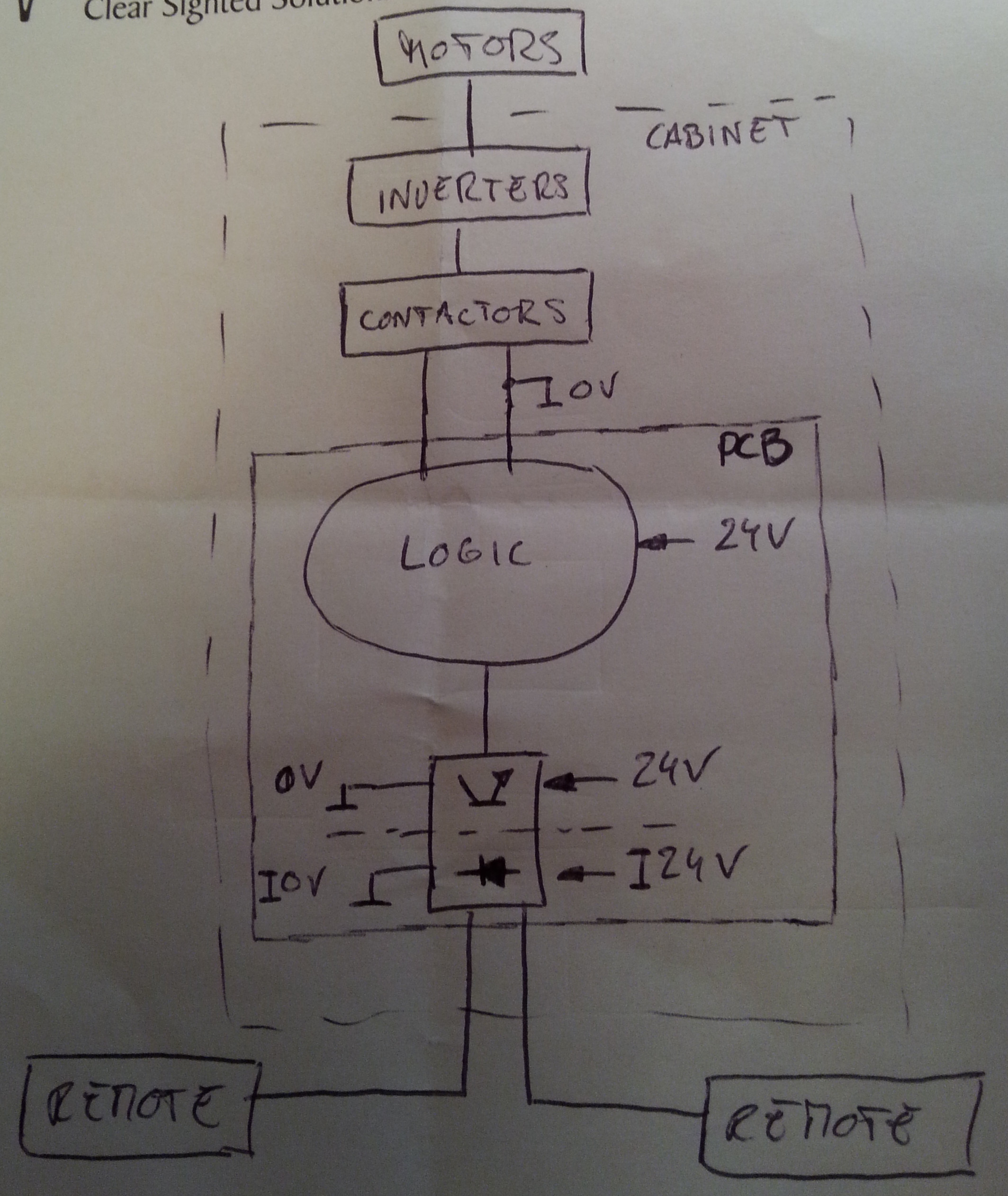
I have got a PCB with two separated blocks, with independent power supplies and I/O connectors in both sides.


Gnd in the picture is chassis ground. It will converge with the other two pcb grounds (0V and I0V) close to the power input connectors, and from that point a single wire will connect with system chassis.

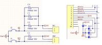
I know that each TVS diode should be placed close to the connector and give it a low inductance path to ground.
But my question is...which ground? Surge currents should be conducted to chassis, shouldn't they?

I will have solid internal ground planes for 0V and I0V, and I was thinking of create another plane on external layer for chassis ground and use it to tie all TVS's directly to it...something like this:


Regards
 

Its not good idea to have so many ground plane. You can provide chasis ground for TVS. However if you want to isolate IO GND and GND then use ferrite beads.
 

You wont get proper return path for the signals which is running above GND layers.
 

Do you mean in case of signals referenced to I0V, but running over 0V plane for example?
 

If you make different GND ice lands, then signal will flow from one ground plane to other. In that case return current path has to go through plane splits which may cause signal integrity issues.
 

I already had in mind not to make signals go through plane splits.
I believe I will be able to treat my board as if it were two separate boards, running every signal only above the plane it is referenced to.
 

What is going to be on the I0V and 0V how are they going to be related etc..... what signals are you running, speed analogue digital etc.
Is it a mixed signal board, is there high current etc. etc.
Can you avoid capacitive coupling etc.
 

What are you wanting to protect?

1) OVP on each supply from line surges?
- Then apply TVS or MOV direct to each PS at source with polyfuse in series.

2) OVP on signals on cables from EMI transients to prevent CMOS latchup? e.g. ESD
- then apply TVS to signal and signal ground close to cable input.

3) ESD ground shift causing CMOS latchup?

Where/how is earth , IO cables and PCB ground connected to case? or is it isolated? ESD transients can be capacitively coupled and CM chokes on cables can attenuate 10ns pulses.

Please see the diagram below


The board contains a 24V logic block made of optocouplers. No CMOS, nor digital stuff.
It has some isolated IO (this is what I want to protect), connected to some remote switches through long cables. These cables are shielded and the shields will connect to cabinet chassis.
The shields connection to chassis must be done at the enter point of the cable to the cabinet, am I right?

I am trying to distribute and route IO and logic elements in a way which allows to have a whole section in one side of the board and the other section in the opposite side, so I can treat them as two separated boards, with solid power and GND planes. Both GND planes will join at power input.

But I do not know if it is a good practice to add a chassis ground to the board too and tie the TVS's to it.
The PCB will be connected to chassis using a wire connected to one of the mounting holes (close to power input).
Some of the TVS's are placed at the opposite corner of the point where the chassis wire will be connected. So, if I tie them to IO GND and an ESD happens, the current will go through the entire board to reach the chassis and earth, am I right?


Thanks
Jose
 

The protection loop wants to be as small as possible, with the return straight to the connector or chassis by the shortest route possible, broadside routes here will also help.... Signal over return for tightest inductive path possible.
 

Ok I understand.
But, for example...If I have a remote switch connected to the board through a shielded twisted pair (shield connected to chassis) and a surge occurs on the cable...
Does the surge current want to reach earth if a proper path is given?
In that case...As the cable shield must be connected to chassis at cable enter point to it...is a good practice using the cable shield to make current runs to earth from the board if we connect the shield to the board connector too?
 

I think that the grounding arrangement should be designed separated in stages, each one comprising components within specific rooms. For instance, all surge protection devices should be placed over a power gnd near to board connectors, so that shielding of cables, as well equipment chassis would be directly connected at this potential. In other hand, inner analog and digital signals should be placed at their respective grounding and if needed a metal plate or a metal case to provide additional EMI shielding, this should be tied to the inner analog/digital ground. In shorts, you should consider split the ground at one purposed to rough protection and another purposed for shielding.
 

Status
Not open for further replies.

Part and Inventory Search

Welcome to EDABoard.com

Sponsor

Back
Top