Continue to Site

Welcome to EDAboard.com

Welcome to our site! EDAboard.com is an international Electronics Discussion Forum focused on EDA software, circuits, schematics, books, theory, papers, asic, pld, 8051, DSP, Network, RF, Analog Design, PCB, Service Manuals... and a whole lot more! To participate you need to register. Registration is free. Click here to register now.

MOSFET Bridge giving power loss even with zero load.

Status
Not open for further replies.

mrinalmani

Advanced Member level 1
Joined
Oct 7, 2011
Messages
463
Helped
60
Reputation
121
Reaction score
58
Trophy points
1,318
Location
Delhi, India
Activity points
5,285
Am MOSFET inverter (H-Bridge) is giving power loss of 4W even without a load.
The details are given below:
V = 12V
F = 100KHz
MOSFET Rds = 1mOhm

The gate input to all the MOSFETS are absolutely clean with almost no overshoot, gate voltage is 10V.

When I connected only the lower two MOSFETs, and gave the input signal, the current drawn by the 12V battery was 90mA, including driver current.
When I connected the upper two MOSFETs also, the current increased to 350mA (average).
I have also blown off a few upper MOSFETs by over heating.

Oscilloscope readings show pulse current as high as 15A during switching. However, there is little possibility of shoot-through as the dead band is 1uS and driver rise time is only 185nS.
Also since the internal resistance is only 1mOhm, even a continuous 15A would cause negligible heating, forget about pulses. Some where or the other both voltage and current are occouring simultaneously. But why? There doesnt seem to be a good reason... Where is this current pulse arising from?
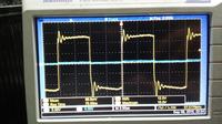
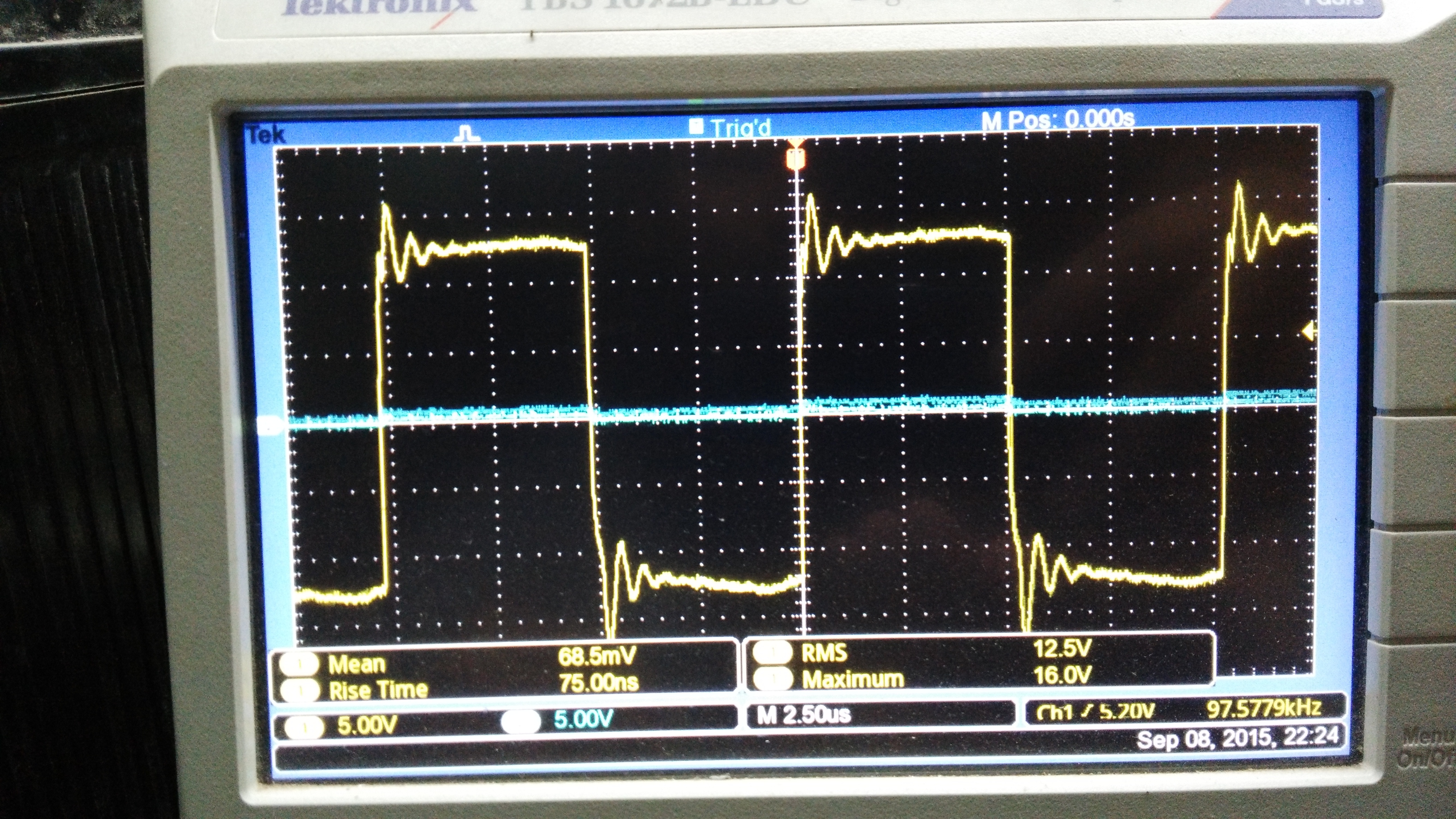

(Output waveform)

IMG_20150909_000825.jpgIMG_20150909_000825.jpg
(Voltage blue, current yellow)

Please help!
 

Hard to say when you doesn't reveal your design.

In general I suspect this to be a result of dynamic losses (increases with higher frequency).

What is the rating of your inverter? 4W in losses doesn't seem much to me.
 

there is little possibility of shoot-through as the dead band is 1uS and driver rise time is only 185nS

Did you try increase the dead time a few more ?
The title of the thread suggest this as a plausible cause.

If there is no current flowing through the load, it can only be dissipated in the bridge itself.
 

I am beginning to suspect Cdv/dt shoot through.
I think when the upper MOSFET switches on, the drain of the lower MOSFET becomes 12V. The Drain-Gate parasitic capacitor must charge to 12V. And this charging current flows through Cgs.
Solution of differential equations with suitable parameters shows a gate spike of nearly 5V in the lower MOSFET.
I will check gate spikes on oscilloscope and also place a 10nF capacitor across the lower MOSFETs to provide a bypass path for charging of Cds.
 

It's normal operation to get a certain amount of switching losses at zero load current in a hard switching bridge, mainly during charging the output capacitance of the opposite transistor. You need to consider the non-linear output capacitance to calculate the respective losses correctly.

About 1W losses per transistor is however a lot, what's the transistor type.

To exclude dv/dt induced turn-on, you can use asymmetrical gate drive with a diode-resistor combination.
 
Voltage spike of 3 to 4V for around 300ns on the gate terminal of the lower MOSFETs has been confirmed on the oscilloscope, each time the upper MOSFETs switch on.
This means that each time the upper MOSFETs switch on, the lower MOSFET on the same leg also triggers for a few nano seconds.
4W loss is certainly NOT due to discharging of output capacitance. Calculations show that at 12V, 100KHz, loss due output capacitance would be less than 200mW.
The loss is probably due to Cds*dv/dt current finding its way through the gate-source capacitor.
The MOSFET type is: NXP PSMN0R9-25YLC: 25V, 100A, 0.75mOhm, logic level gate.
This logic level gate is adding up to the problem.

Asymmetrical drive with a diode-resistor combination?
The bottleneck is the P type gate driver MOSFET, if I bypass the external gate resistor by a diode, it may not be able to handle such repeated pulses.
What is the standard way of driving hard switched bridges?
 

The bottleneck is the P type gate driver MOSFET, if I bypass the external gate resistor by a diode, it may not be able to handle such repeated pulses.
I don't understand the problem. It's quite normal to drive gate drivers into saturation during switching edges, And you don't necessarily need to bypass the gate resistor, you can use RRD circuit,

Asymmetrical gate drive is pretty standard, also to peak currents during switch-on and reduce EMI.
 

The datasheet of the driver MOSFET states maximum pulse current of 2.1A. Therefore I was concerned about bypassing the resistor.
I did a google search for asymmetrical drivers, went through a couple of datasheets as well. What I understood is that asymmetrical drivers have higher sink capability than source capability.
Is that what you meant by asymmetrical driving?
Sorry, but I did not understand RRD circuit. What does it stand for?
 
Last edited:

Just came across an application note from Infineon.
It says not all MOSFETs are intended for bridge application, regardless their low internal resistance and gate charge.
For reliability issues, MOSFETs used in bridge or similar application must have a ratio of Cgs/Cgd > 15 , otherwise they are likely to fail due to Cdv/dt shoot through.

For my MOSFET the ratio was approx 10.
I came across several MOSFETs designed especially for bride and similar application.

Toshiba TPWR8004PL,L1Q (Ratio =125)
TI CSD17559Q5 (Ratio = 80)
Infineon BSC010N04LS (Ratio = 41)

All these MSOFETs are of nearly 1mOhm with current capability > 100A
 

If you compare capacitance ratio for low Vds values, e.g. 5 V, they are less apart.

Low reverse transfer capacitance is surely a point to consider, but it's unlikely to be an essential parameter for low voltage bridges. I still believe the problem is unsuitable gate control.
 

I agree your Gate driver impedance may needs to be as low as 50x~200x RdsOn for fast switching off time and Diode reverse recovery time needs to be equally fast for inductive loads.

This is my rule of thumb for controlling shoot thru with cascaded complementary drivers, being the RdsOn ratio of successive stages. The lowest cost-effective Ciss * RdsOn is a figure of merit I also use for choosing suitable devices.

turn off time ( delay + fall time) are also important to compare your driver with one used in test spec.
 

Well, I tried the following
1. RRD driver: Doesn't really help much because even if diode bypasses the gate resistor, the internal resistance of P type MOSFET is high enough to cause problems.
2. Replaced MOSFET with TI CSD17559Q5. This has a high Cgs/Cgd ratio. It helped reduse losses from 4W to nearly 1.5W. But still not a permanent solution.

I'll order a different board with enhanced driver configuration, but no more of NP type drivers anymore for bridge configuration. I'll use NP types only in independent switch configuration.

The problem is that logic drive power MOSFETs are triggered easily at 1.5V, this is close to the threshold voltage of the P MOSFET in the driver which is around 1V. Even half a volt glitch triggers the power MOSFET.
I have designed NN type drivers which will clamp the gate voltage to 0V and not keep it semi-floating at 1V. This will keep the driver resistance well in the range of 200x of Rds_on.
Have simulated this and it appears to be absolutely glitch free.
Meanwhile I have ordered MOSFETs with Vth in the range of 3V as opposed to 1.5V of all previous MOSFETs
Will post result soon...
Thanks for help
 

The problem is that logic drive power MOSFETs are triggered easily at 1.5V, this is close to the threshold voltage of the P MOSFET in the driver which is around 1V. Even half a volt glitch triggers the power MOSFET

Why don’t you consider using a driver circuit configuration that supplies negative Vgs(low) voltages ? These topologies are pretty suitable for MOSFETs having so small threshold voltage, keeping them away from conduction region, being particularly beneficial to avoid leakage surges across Cgd during cut-off transitions.

Take a look at the picture 21 of this AN which could give you some insight:
 
Status
Not open for further replies.

Similar threads

Part and Inventory Search

Welcome to EDABoard.com

Sponsor

Back
Top