Continue to Site

Welcome to EDAboard.com

Welcome to our site! EDAboard.com is an international Electronics Discussion Forum focused on EDA software, circuits, schematics, books, theory, papers, asic, pld, 8051, DSP, Network, RF, Analog Design, PCB, Service Manuals... and a whole lot more! To participate you need to register. Registration is free. Click here to register now.

Problem with Vds voltage at MOSFET

Status
Not open for further replies.

madhu.b

Member level 3
Joined
Sep 25, 2011
Messages
66
Helped
1
Reputation
2
Reaction score
1
Trophy points
1,288
Activity points
1,846
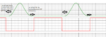
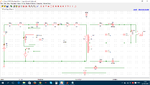
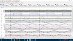
I am working class-E DC-DC converter topology. I have the problem with the drain-source voltage which is not immediately start to rise the Vds voltage after the gate voltage zero. So, what are the values need to tune in order to get the ZVS (zero voltage switching). I can get it at another side. See, the attached Vds file.
 

Attachments

  • Vds.png
    Vds.png
    23.4 KB · Views: 103
  • Class-E Circuit.png
    Class-E Circuit.png
    54.8 KB · Views: 106
  • Class-E Simulations.png
    Class-E Simulations.png
    75.3 KB · Views: 144

Hi,

I think it is because of the current flow.

Show Charts for I_L1, I_C1, I_Source and I_C8.

Klaus
 

AS RdsON goes lower in MOSFETS CIss and Coss increases. If your series cap is small compared to this, then the impedance ratio at this frequency will determine the response time THus if resonant , smaller L bigger C in the buck boost resonant circuit. or change the MOSFET with better FOM for RdsOn*Ciss

FOM is a designers figure of merit, you calculate on selection criteria and compare with cost and other requirements.
 
Thank you Sunny,

But, I have another question...

If, I would like to work with the same MOSFET in the converter. What I have to change in the circuit and which values I have to tune. Because the MOSFET specification is matches to my work specification and also other hand the Vds voltage and Id current is more high which will helps in the real time work, even If the circuit runs with the hard switching condition. So, the MOSFET has less changes to burn out if I use this MOSFET.
 

My best guess is the strange shape of Vds is due to the nature of that particular GaN FET. Its datasheet shows a turnoff delay of 33ns, and the Coss is incredibly nonlinear. This means the rise of Vds should be somewhat sluggish. Hard to tell if it's reasonable since you don't show the time axis in your waveforms.
 
Last edited:

Status
Not open for further replies.

Similar threads

Part and Inventory Search

Welcome to EDABoard.com

Sponsor

Back
Top