Continue to Site

Welcome to EDAboard.com

Welcome to our site! EDAboard.com is an international Electronics Discussion Forum focused on EDA software, circuits, schematics, books, theory, papers, asic, pld, 8051, DSP, Network, RF, Analog Design, PCB, Service Manuals... and a whole lot more! To participate you need to register. Registration is free. Click here to register now.

Is this H bridge going to work properly?

Status
Not open for further replies.

Boky

Newbie level 4
Joined
Aug 30, 2014
Messages
5
Helped
0
Reputation
0
Reaction score
0
Trophy points
1
Activity points
59
Hello everyone :)

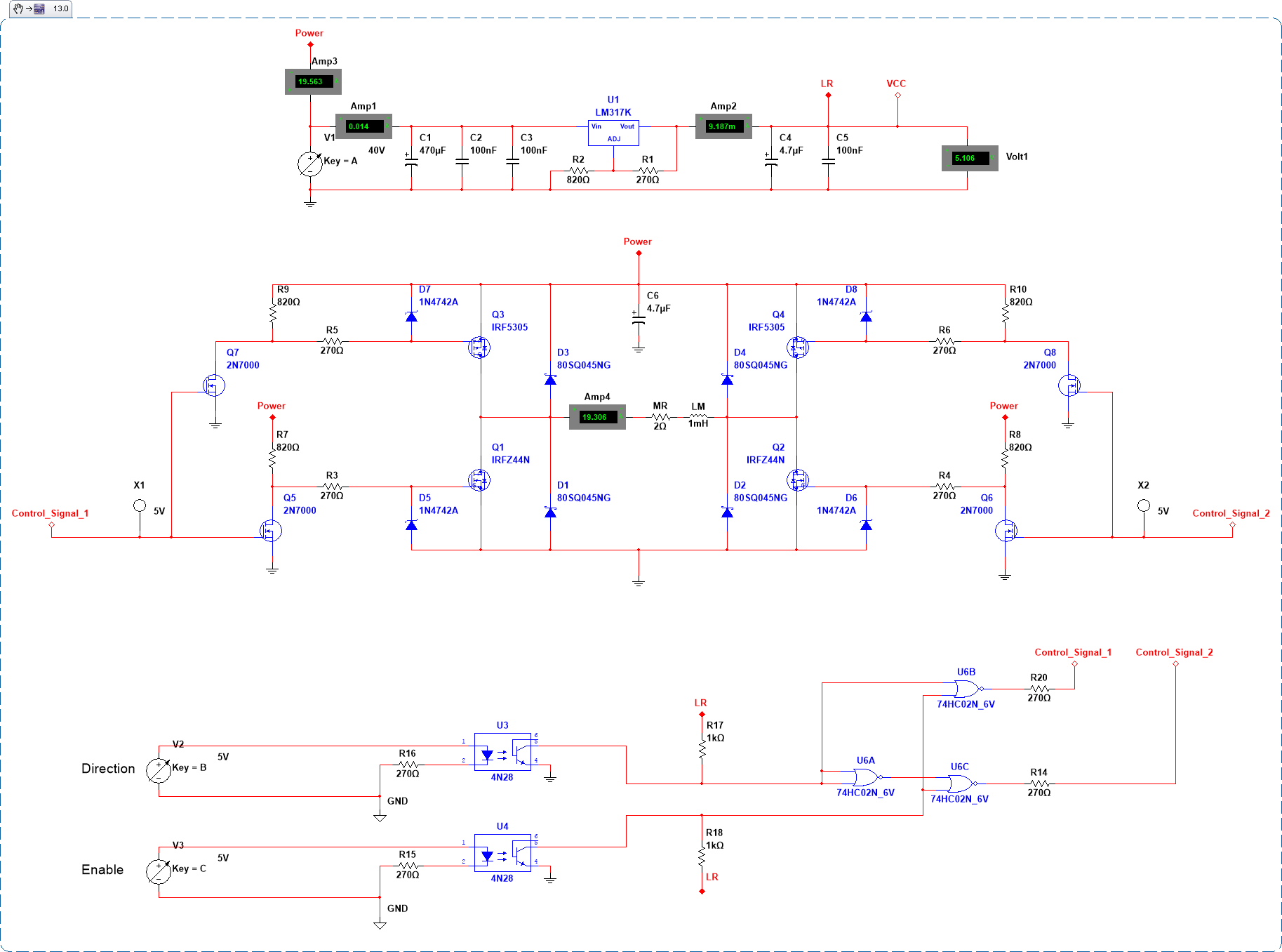
I have one question. I think that this design on picture should work, but I am not sure because when I change direction signal from high to low or vice versa simulation program gives me an error, now I am not sure is this design going to work in real life?

Also is it possible to control speed of motor with this H bridge by applying PWM signal to enable pins?


Best regards
 

Attachments

  • High Power H bridge.png
    High Power H bridge.png
    361.2 KB · Views: 132

Looks to me like you are driving both transistors on each side at the same time instead of 'crossing over' the drive signals diagonally. I think it will work, but only for one PWM cycle before burning out !
You also have no dead-band period and I suspect the transistors will not have sufficient Vgs to full turn on.

Brian.
 

Thank you for your reply and help.

if you want to simulate this circuit by yourself in Multisim simple open schematic image in new tab (https://obrazki.elektroda.pl/6711453500_1439313836.png) and then just drag and drop it in empty multisim worksheet.

When control_signal_1 is +5V control_signal_2 is 0V so only diagonal power mosfets are turned ON by 2n700 signal mosfets (Q1 and Q3) while other two power mosfets (Q2 and Q4) are turned OFF. Direction signal change will reverse it so control_signal_1 will become 0V and 2 will be 5V

2n700 mosfet is able to turn on at 5V signal according to datasheet.

Yes I have also thought to drive those mosfets from 4 idependent signals and I have simulated that too but with same results.

All in all it I think that this is horrible H bridge design it seems that it is really hard or maybe impossible to create H bridge which can work up to 40V without hi/lo side mosfet driver.

I will try to create somehow dead-band period and see if that solves problem.

Best regards
Bojan.
 

Status
Not open for further replies.

Part and Inventory Search

Welcome to EDABoard.com

Sponsor

Back
Top