Continue to Site

Welcome to EDAboard.com

Welcome to our site! EDAboard.com is an international Electronics Discussion Forum focused on EDA software, circuits, schematics, books, theory, papers, asic, pld, 8051, DSP, Network, RF, Analog Design, PCB, Service Manuals... and a whole lot more! To participate you need to register. Registration is free. Click here to register now.

Please explain this BJT circuit to me

Status
Not open for further replies.

muheeb16

Member level 3
Joined
Jul 18, 2015
Messages
55
Helped
1
Reputation
2
Reaction score
1
Trophy points
8
Activity points
416
I have always found it very easy to design with dual supplies.This circuit uploaded by me is operating in active region because Vec=3V.Mostly in such circuits very negligible base current flows (don't know why).I find this very strange because the base current controls the collector current.On the contrary if I replace the negative battery (on the bottom right) with ground very large base current starts flowing.I can not understand why? sim1.PNG
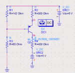
 

.I find this very strange because the base current controls the collector current.View attachment 119990

Perhaps your problems are reduced - and your understanding of BJT circuits improved - if you are able to accept that the BJT is NOT a current-controlled device. Instead, it can be easily shown and prooved that the BJT is voltage controlled (Ic is controlled by VBE). I am aware that in some books you can read the opposite.
That is one of the myths I do not understand: More than 60 years after the BJT was invented, there are still two different (and conflicting!) descriptions of the BJTs working principle.
But believe me - the voltage Vbe determines the value of Ic (and also of Ib, because Ib is a more or less fixed percentage of Ic). Why should a pn junction within the BJT have other properties than within a simple diode?
 
Last edited:

I replace the negative battery (on the bottom right) with ground very large base current starts flowing. I can not understand why?

Suggestion. Measure all circuit voltages and currents and notice the basic change between both operation points. Pay attention to transistor Vce. Calculate the ratio Ic/Ib in both cases and compare with expected current gain.
 

Pay attention to transistor Vce. Calculate the ratio Ic/Ib in both cases and compare with expected current gain.
Without the negative battery at collector the transistor is in saturation and a large Ib makes much sense.But the with battery operation gets me confused.The transistor operates in active region with Vec=2V but Ic is not equal to hFE*Ib.Ib is very low and that is what I cannot understand.
 

Without the negative battery at collector the transistor is in saturation and a large Ib makes much sense.But the with battery operation gets me confused.The transistor operates in active region with Vec=2V but Ic is not equal to hFE*Ib.Ib is very low and that is what I cannot understand.

Whar is your problem? Which value do you expect for IB and what is the actual value?
 

Which value do you expect for IB and what is the actual value?
I expect Ib to be Ic/hFE (while its much lesser than this value) because bjt is clearly in active region with Vec=3V
 

I expect Ib to be Ic/hFE (while its much lesser than this value) because bjt is clearly in active region with Vec=3V

Yes - correct expectation. And...? What is the value of Ib? What is Ic?
 

I expect Ib to be Ic/hFE (while its much lesser than this value) because bjt is clearly in active region with Vec=3V

When you do not follow design guidelines for normal switch non-linear operation, you can expect unusual results.

The BJT has operated as expected because your base bias current far exceeds your load current.

When your bias current is chosen to be much lower than expected operating current with higher value resistors you will not see the same unexpected result. If you expect it to saturate, use base current of 10% x Ic using Ohm's law for bias points.

The current gain will reduce from hFE to 10% of hFE when saturated, typically. Although this is not specified as such, they use Vce(sat) @ Ic for Ic/Ib=10 (typically) and increase this ratio up 50:1 for very low saturated devices , which are specially designed for such operation. ( cost more$)

In your design , Rb bias resistors, should be chosen such that Ic/Ib=10 to get normal expected results. But instead you have the reverse and your bias current is more than the load current. Thus when since it saturated the collector Vcb is starting to get forward biased like Vbe and it takes some of the bias current to feed the emitter resistor current so Ibe reduces the collector comes out saturation.

So change your bias resistor impedance from 50//142 to Rc*10 = 400*10=4k or less
so if you wanted same Vb voltage it could be 5k//14.2k ~ 3.7k
 
Status
Not open for further replies.

Part and Inventory Search

Welcome to EDABoard.com

Sponsor

Back
Top