GilchristT
Newbie level 2
Hi folks.
This is my first attempt at a four layer board and first board involving high speed signalling (USB 3.0).
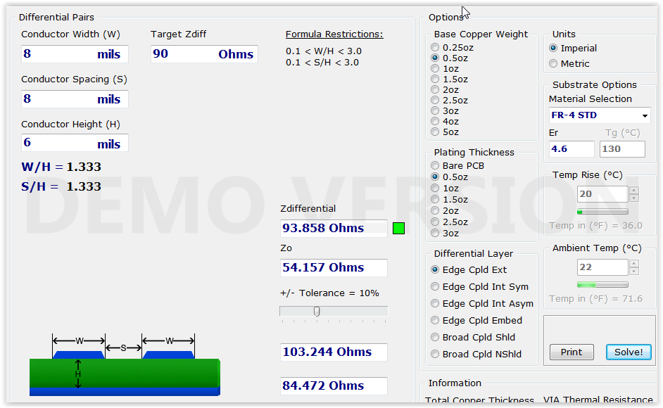
The spec sheet for my USB 3.0 hub component (TSUB8020B) recommends controlled impedance of 90Ω +/- 10%. I've plugged these figures into Altium and it's recommending track widths of 0.036mm (about 1.4mils). The board house I hope to use (Elecrow) can only go to 6mils with 8mils recommended so I've either got my board setup wrong or need to go to a significantly better board house?
This is also my first attempt at defining a proper layer stack and could very likely have made a mess of it. I just picked the Altium template for a four layer board.
Can anyone advise if I've gotten something configured wrong or if these figures are realistic?
Thanks
Tommy


This is my first attempt at a four layer board and first board involving high speed signalling (USB 3.0).
The spec sheet for my USB 3.0 hub component (TSUB8020B) recommends controlled impedance of 90Ω +/- 10%. I've plugged these figures into Altium and it's recommending track widths of 0.036mm (about 1.4mils). The board house I hope to use (Elecrow) can only go to 6mils with 8mils recommended so I've either got my board setup wrong or need to go to a significantly better board house?
This is also my first attempt at defining a proper layer stack and could very likely have made a mess of it. I just picked the Altium template for a four layer board.
Can anyone advise if I've gotten something configured wrong or if these figures are realistic?
Thanks
Tommy