Continue to Site

Welcome to EDAboard.com

Welcome to our site! EDAboard.com is an international Electronics Discussion Forum focused on EDA software, circuits, schematics, books, theory, papers, asic, pld, 8051, DSP, Network, RF, Analog Design, PCB, Service Manuals... and a whole lot more! To participate you need to register. Registration is free. Click here to register now.

Need some feedback on my SMPS design

Status
Not open for further replies.

twenglish1

Junior Member level 1
Joined
Aug 1, 2015
Messages
16
Helped
0
Reputation
0
Reaction score
0
Trophy points
1
Activity points
145
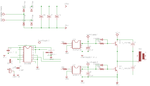
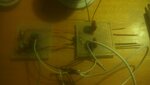
I am currently working on designing and will be building my own switch mode power supply, i will be starting out with a lower power one of similar design just to learn the basics, eventually i will be ramping up the power and trying to build a 4000 watt or so welding power supply. Currently this is what i have drawn up, i need to ask how do i calculate the values of the C7 and C8? Does anybody see any problems with my design so far? or any suggestions on what should be done differently?
 

Attachments

  • SMPS.png
    SMPS.png
    17.4 KB · Views: 88

Hi,

It depends on frequency and load current.
Calculate it to be 10% ...20% of load voltage.

Consider to change 1N4004 into UF4004

Klaus
 

What should the capacitance be for C7 and C8? I have been doing lots of reading and that is one thing I can't seem to find any information on, and Frequency will be around 40 - 50khz, and I should have mentioned those aren't the igbts I will be using, I will be using a half bridge igbt brick, Toshiba MG150Q2YS40, just used those since I didn't have the actual part in eagle
 

MG150Q2YS40 specifications are based on a bipolar +/- 15V gate drive with 5.6 ohm gate resistor, considerable different from what you have planned. It's however a 150 A IGBT module and good for several 10 kW, a bit oversized for a 4 kW inverter.
 

I understand that they are oversized, I scored a box of them for a very good price so decided I would make some use of them, once i learn more of the basics and get some working power supplies done I plan to build more powerful ones, and eventually I would like to try a full bridge and a 3 phase motor driver. Would I need to build a driver that provides +/- 15v for these IGBT modules?
 

From your schematic, C7 & C8 will each charge to 1/2 the supply voltage. Thus each will have 120V.

Your power spec is 4000W. Then the capacitors will have 33A going back and forth through them (average).

The aim is for the charge not to go down too much during the time when it is providing power. Suppose we allow ripple to be 10%. This is during a half cycle at 40 kHz.

A simulation shows they can have a value of 20-30 uF, to fulfill these operating parameters.
 

Ok thank you that makes sense, what is the best type of capacitor to use? I have read a lot of mixed reviews on the subject, some say elecrolytics are fine and others have said that the high frequency isn't good with them, and film caps should be used, also heard that under 100khz electrolytics are acceptable to use, could anybody provide some more input on the type of caps to use?
 

To choose a suitable type of capacitor, first picture 33 Amperes going back and forth through it, many times a second. You can be sure you'll need something very robust.

It needs to have very low ESR.

It should be rated for the maximum voltage it might be exposed to. Normally it is 1/2 the supply voltage. However if something were to go wrong with the switching signal, so that it locks hi or low, then one transistor would stay on and the other would stay off. Then one cap would charge to full supply voltage, possibly a peak of 330V.
 

Won't the caps also see voltage spikes from the switching of an inductive load such as a transformer? I have read some about adding snubber caps, I see they are usually designed to bolt right to the igbt module, how is the value of the snubber cap selected? If I understand correctly snubber caps are for absorbing these voltage spikes from an inductive load right?
 

Although spikes are likely, it's also possible they will be absorbed by C7 & C8.

Nevertheless it is still a good idea to add some snubber network. It might be a capacitor, or cap & resistor in series, etc. As for their values, the idea is to absorb a spike of the amount of Amperes (33A) during which it lasts. It will last a small fraction of a cycle (40kHz). I guess it will contain a certain number of joules, which provides the basis for calculating the value. But you'll probably find experimentation is just as helpful to determine what values make an effective snubber.
 

Film caps across the electro's is a good idea as they handle most of the switching currents and allow the electro's to "catch up" due to their ESL & ESR...
 

I will look into ordering some different snubber caps to try, also I know that it is important to keep the wires between the bulk cap bank and the igbt and the transformer as short as possible to minimize stray inductances, I will post some results, I currently have the sg3525 circuit completed and I am waiting on the hcpl3120 ics and the two 15 volt power supplies
 

You have already C7 and C8 as low ESR, high current film capacitors. Why would you need additional snubber capacitors parallel to the main bus capacitors?

Assuming that the high frequent output current is mainly sourced by C7 and C8, each capacitor is loaded with a half-have, corresponding to 23,5 A Irms each. You most likely need a parallel circuit of multiple high current capacitors (e.g. Kemet R73, Wimi MKP10) to handle the current.

Regarding capacitor sizing, one option is to establish a series resonant converter with C7||C8 and transformer leakage inductance.

Bipolar versus unipolar gate drive, I just wanted to mention that high current IGBT are ususally expected to use bipolar gate drive. This doesn't mean that unipolar isn't feasible, but you actually need to optimize switching parameters, not just copy and past a gate driver circuit from a low power application. I also think that HCPL3120 is on the lower edge of required gate current.
 

I will look into those mentioned capacitors, and about the driver circuit, I chose the hcpl3120 because I saw a guy experimenting with them on YouTube driving similar igbt modules at very high powersand he had very good results, he also just used a 555 timer, I have looked into using something like an ir2110
 

HCPL3120 is surely better than IR2110. The output current should be still suffcient for your IGBT modules, it's also suited for bipolar gate drive if used with a respective power supply, IR2110 isn't.
 

I looked into the ir2120 and other similar drivers to avoid using a separate supply for the high side, however I found on eBay some small 15v switchmode supplies for around $6 a piece, not sure on quality, but I will give them a try, if I get good results I will order two more so I can do bipolar drive, to get faster turn off times, the reason why I added the diode in parallel with the resistor so the gate doesn't have to discharge through the resistor, as a cheap way to try and increase the turnoff time but with bipolar drive I should be able to get even faster turn off times
 

Adding on to the last post I made, did not see an edit button, anyways, was thinking more about my undersized specs for the igbt modules i will be using, I mentioned I will be using ee80 ferrites, I understand that I can parallel multiple sets of cores to make a higher powered power supply, how could I calculate how much power is feasible with a single ee80 core with the half bridge inverter topology? I think I read somewhere roughly 5kw? Is that anywhere close?
 

At 4kW you will have around 26A rms in your input bridge rectifier, this will give about 43 watts of heat so make sure it is on a good sized heatsink. 4kW is a pretty big design challenge - even for your relatively simple approach, turning IGBT's on too fast will lead to RFI getting into your control and gate drive causing problems, and diode turn off spikes can do the same. If you get it built run it up slowly, as inevitably, at some power level there will be problems, it is also very easy to kill your o/p diodes with narrow overvolt spikes...!
 

Are there some simple methods of rfi blocking for the control circuitry? That is one aspect I haven't though alot about, wasn't sure how big of a problem it would be at 40khz? Another question I had is about the sg3525 circuitry, would there be a way to change that portion of the circuit around so I could directly vary the duty cycle and keep the frequency stable?
 

Here is an update: Just finished building the driver circuit, square waves are transfered perfectly between the SG3525 to the HCPL3120 ics, and i am waiting on the 15v power supplies, attached a picture of the boards, and a scope output, showing turn off of a, dead time and turn on of b, measured from the hcpl3120 outputs powered by single power supply for testing
 

Attachments

  • IMAG2833.jpg
    IMAG2833.jpg
    831.5 KB · Views: 55
  • IMAG2831.jpg
    IMAG2831.jpg
    1.1 MB · Views: 48

Status
Not open for further replies.

Similar threads

Part and Inventory Search

Welcome to EDABoard.com

Sponsor

Back
Top