sanketpatel2020
Newbie level 4
Hi! Greetings!
I am used to generate mictrostrip to layout and then export to gerber in ADS.
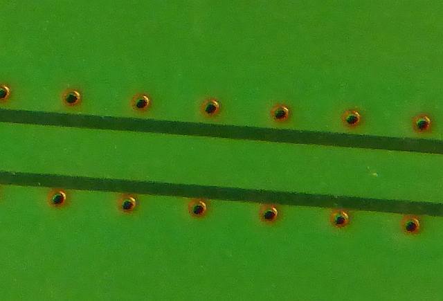
However, I am first time dealing with CPWG lines. I can see CPWG converted in the layout with center conductor (line width W) and thin ground lines at distance (Gap=G) apart.
I can see the same once I export the layout to gerber.
However my doubt is why the outer ground lines are so thin and not the typical PCB layout lines where we have center conductor and a gap, and a ground everywhere else (the way it should look like as shown in the attached image "Expected").?
Please guide me in this regard.
what_I_am_getting:

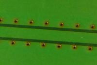
Expected like this:
I am used to generate mictrostrip to layout and then export to gerber in ADS.
However, I am first time dealing with CPWG lines. I can see CPWG converted in the layout with center conductor (line width W) and thin ground lines at distance (Gap=G) apart.
I can see the same once I export the layout to gerber.
However my doubt is why the outer ground lines are so thin and not the typical PCB layout lines where we have center conductor and a gap, and a ground everywhere else (the way it should look like as shown in the attached image "Expected").?
Please guide me in this regard.
what_I_am_getting:

Expected like this: