Ahmedsalim789
Junior Member level 1
Hi
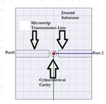
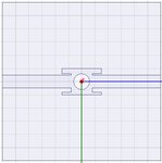
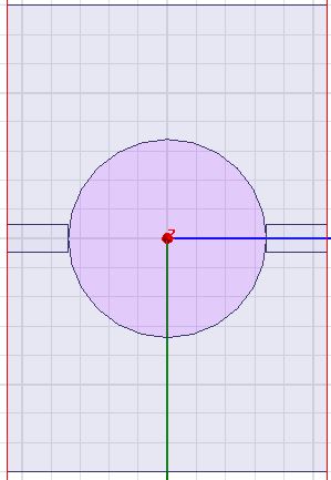
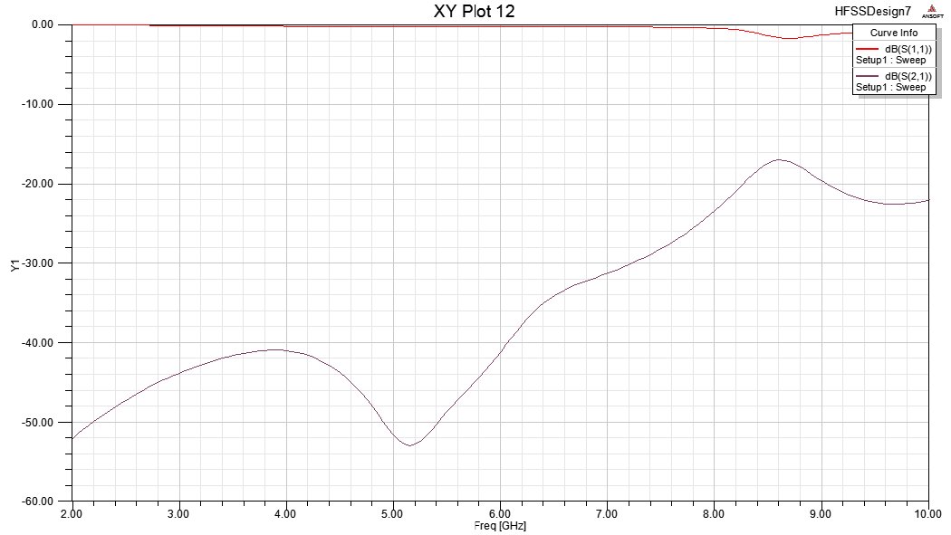
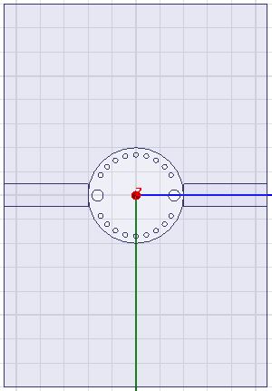
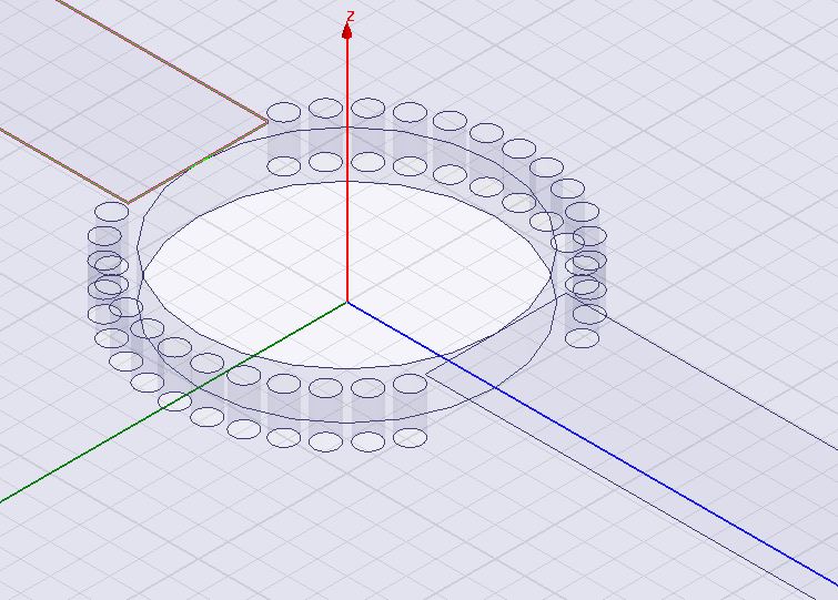
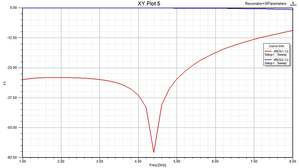
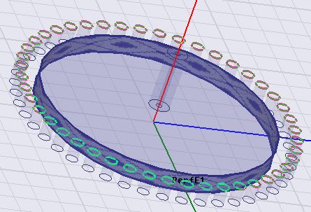
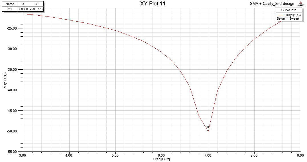
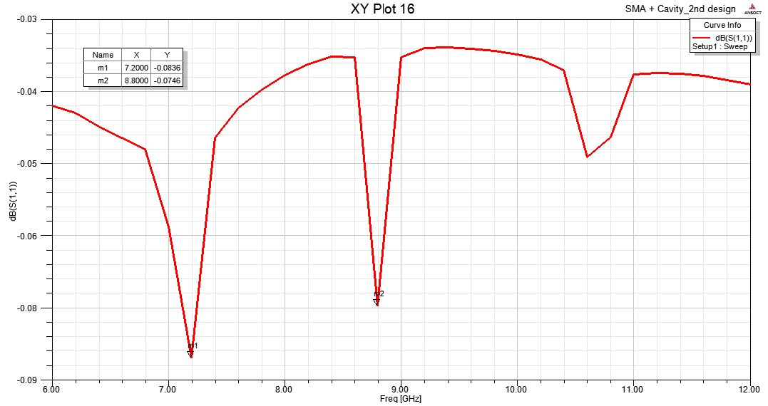
I designed a cylindrical cavity resonator but the structure is not resonating. I used the idea of microstrip line for excitation through two wave ports.
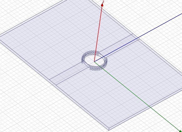
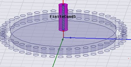
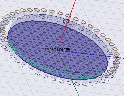
As another option for excitation of cavity resonator, I thought to place a patch of Copper on top side of cavity and this patch is given an inset feeding. But It did not work yet.
Please help me.
Thanks
I designed a cylindrical cavity resonator but the structure is not resonating. I used the idea of microstrip line for excitation through two wave ports.
As another option for excitation of cavity resonator, I thought to place a patch of Copper on top side of cavity and this patch is given an inset feeding. But It did not work yet.
Please help me.
Thanks