Continue to Site

Welcome to EDAboard.com

Welcome to our site! EDAboard.com is an international Electronics Discussion Forum focused on EDA software, circuits, schematics, books, theory, papers, asic, pld, 8051, DSP, Network, RF, Analog Design, PCB, Service Manuals... and a whole lot more! To participate you need to register. Registration is free. Click here to register now.

[SOLVED] Altium Designer: Errors Polygone connect

Status
Not open for further replies.

yokohama

Member level 3
Joined
Dec 29, 2010
Messages
55
Helped
4
Reputation
8
Reaction score
4
Trophy points
1,288
Location
Algeria
Activity points
1,659
Hi, everybody.
Polygone connect.png
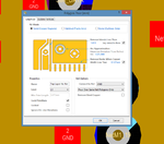
On the picture above you can see that I have 3 GND SMD pads. The right one is connected directly to the polygone and the two on the left aren't directly connected to the polygone.
Why ?. I remember that I've set the parameter PolygonConnect to 'Direct Connect' on the Design Rules.
Thank's for your answers.
 

Change the "Pour over same net polygons only" setting to "Pour over all same net objects" under that polygon's settings. (See your second image.)

Also, the polygon clearance from GND shown in the first image looks weird since it appears to only be creating clearances from the trace and not the pads. The other net clearances look reasonable, so the problem may just be a result of your various attempts to fix your original problem. If so, you will want to revert some of the changes you made to the clearance rules as you were attempting to troubleshoot your polygon problem.
 
Yes man; that's exactly what happend. I forgot the 'Pour over all same net objects'.
Thank's again.
 

Status
Not open for further replies.

Part and Inventory Search

Welcome to EDABoard.com

Sponsor

Back
Top