Continue to Site

Welcome to EDAboard.com

Welcome to our site! EDAboard.com is an international Electronics Discussion Forum focused on EDA software, circuits, schematics, books, theory, papers, asic, pld, 8051, DSP, Network, RF, Analog Design, PCB, Service Manuals... and a whole lot more! To participate you need to register. Registration is free. Click here to register now.

how can i implement this delay element in vhdl?

Status
Not open for further replies.

fahim1

Member level 4
Joined
Jun 4, 2015
Messages
75
Helped
2
Reputation
4
Reaction score
2
Trophy points
8
Activity points
517
hi
i want to write structural code for this serial multiplier and this D block is just defined as an delay element,how can i write synthesizable code for this element???
hgg.PNG
 

The D stands for delay. It is nothing but a flip flop (a DFF).
 

I assume you know how to wire VHDL code for an adder and multiplier. You also now know that a delay element is nothing but a flip-flop (Sarath666's reply above). So create a basic entity containing the adder, multiplier and the delay-element. Later instantiate this entity as many times as you want. Referring to your figure, you need to connect a delay-element between each instantiated basic entity so as to get your desired functionality.
 
  • Like
Reactions: fahim1

    fahim1

    Points: 2
    Helpful Answer Positive Rating
The D stands for delay. It is nothing but a flip flop (a DFF).
in the way u said i should do this multiply in six clks but i want to write this code and put t in a code that execute in one clk/?
how would that possible?
i think its too messy
 

To do it in 1 clock, remove all the delay elements..
 

hi
i want to write structural code for this serial multiplier and this D block is just defined as an delay element,how can i write synthesizable code for this element???
View attachment 118535

in the way u said i should do this multiply in six clks but i want to write this code and put t in a code that execute in one clk/?
how would that possible?
i think its too messy

That highlighted red text should have told you that it wouldn't work in 1 clock cycle.

Have you studied digital design? You're issues seem to be more of a problem with that than with actually writing HDL (ignoring all the typos you post).
 
  • Like
Reactions: fahim1

    fahim1

    Points: 2
    Helpful Answer Positive Rating
That highlighted red text should have told you that it wouldn't work in 1 clock cycle.

Have you studied digital design? You're issues seem to be more of a problem with that than with actually writing HDL (ignoring all the typos you post).

thnx for ur help.
do u know why carry have a feedback with a delay to the same adder block???
 

I'd assume it's an unusual way to draw an accumulate.
 

for adding carry because i think otherwise the carry will be wasted???
 

Oops I wasn't think of a serial multiplier in my previous response, so the loop is to accumulate and the other line is probably a carry to the next stage. Didn't the "thesis paper" have any explanation of the block diagram?
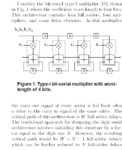
 

Oops I wasn't think of a serial multiplier in my previous response, so the loop is to accumulate and the other line is probably a carry to the next stage. Didn't the "thesis paper" have any explanation of the block diagram?
i didnt found anything.i copied the part of explanation of this adder.
333.PNG

- - - Updated - - -

i think the loop is carry, but i dont know what is the first line below the a0 except the loop?
 

Based on the text the loop is feeding back the carry.

I don't do any serial multiplication in FPGAs as I normally use the DSP hard IP if I need to do any multiplication, so I'm not familiar with the details of serial multipliers.
 

Status
Not open for further replies.

Part and Inventory Search

Welcome to EDABoard.com

Sponsor

Back
Top