Continue to Site

Welcome to EDAboard.com

Welcome to our site! EDAboard.com is an international Electronics Discussion Forum focused on EDA software, circuits, schematics, books, theory, papers, asic, pld, 8051, DSP, Network, RF, Analog Design, PCB, Service Manuals... and a whole lot more! To participate you need to register. Registration is free. Click here to register now.

Regulator driven NPN darlington will not go to 0V, solutions?

Status
Not open for further replies.

David_

Advanced Member level 2
Joined
Dec 6, 2013
Messages
573
Helped
8
Reputation
16
Reaction score
8
Trophy points
1,308
Location
Sweden
Activity points
12,219
Hello.

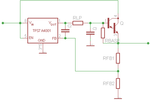
I've been working on a lab supply for some time and I had thought that I had solved how to supply the high current I wanted from a low-noise linear regulator through using a NPN power transistor at its output as this:
REG.png

The low-pass filter is not in use in my prototype, the real circuit are controlled by digital means but the picture above is how my circuits looks like with some modifications to the resistor voltage divider for control of output voltage.

First I had no NPN on the output and everything worked just as thought but when I added that(along with some other modifications to the board) the output when told to go to 0V never goes below 5,5V and I thought something is wrong.
I am not experienced within electronics but what was wrong was my thought that something was wrong.

I read the datasheet to a NPN power transistor(by the way, is "Power transistor" the same as "Darlington transistor"?) and I noticed the Vbe voltage was to be 5V... But that would mean as far as I know that this circuit will never cut it for me and I need to re-think how to get my low-current output low-noise voltage regulator to supply its variable voltage while maintaining a current of 5A. I could adapt the circuit to use the PNP transistor way of boosting a regulators current but I want to ask if there are any way around my problem while still using the NPN design?

Answers I have gotten earlier in other threads on this forum has lead me to believe that its gives me benefits when using my current circuit through the fact that the transistor is within the regulators feedback-loop and as such does not degrade any characteristics, but the PNP way of doing it is does not put the transistor within any feedback-loop and my regulator can only supply 50mA above which the PNP would take over(or is it adding to the already supplied 50mA).

I have not knowledge enough to be able to measure the proposed circuit to detect if it papooses any problems.

Regards

- - - Updated - - -

A possibility would be to ditch the integrated linear regulator circuit and apt for an linear regulator made of transistors and a opamp or any such scheam.
 

First of all, a power transistor may be a darlington, or not. And a darlington may be a power transistor, or not. Secondly, I think you've misread the data sheet: Vbe for the transistor is not 5V. Maybe the MAXIMUM REVERSE Vbe is 5V. Third, what do you mean "told to go to 0V"???? The minimum output of that regulator is 1.2V. You need to show us your actual schematic; don't just post a schematic then tell us what you're REALLY doing is different. You don't show any component values, either.
 

The problem is with the ground and the FB of the regulator chip. the regulator chip always tries to set the FB terminal to +1.25 with respect to the GND pin. So to get the output down to 0V, you need to bias the GND pin to - 1.25V
Frank
 

You have (Rfb1+Rfb2)/Rfb2=4.4. If you want 0V output at the same ratio of resistors GND of regulator must be at -5.5V. I don't think you want this.
 

Sorry, I thought that I manage to tell the problem without full schematic but it appears I might not even know the real problem, anyway here is the schematic. The NPN Darlington has an internal Base-Emitter resistor.

- - - Updated - - -

if you view the image it has real good resolution if you zoom in.
 

Attachments

  • showingSCH.png
    192.3 KB · Views: 116

Your problem, as stated in several posts, is that you can't get zero volts out a part with a minimum output of 1.2V.
 

Your problem, as stated in several posts, is that you can't get zero volts out a part with a minimum output of 1.2V.
The base-emitter drop of the Darlington should be at least 1.2V so I would think the output would go to near zero (with a small minimum load).
 

Hi,

I also think it should go below 1.2V.
The regulators usually don't have the feedback manipulation like here.
The use a voltage divider as feedback. So the lowest output voltage is when there us a feedback from output to fb pin with no resistior to gnd. The min output voltage is then the same as the feedback voltage. Therefir here it is 1.2V.
But with the manipulated feddpack path it should be possible to get an output voltage below 1.2V

Why you see 5.5V is not clear.

What happens when you add a load if 1kOhms? Is it still 5.5V?
Please measure and tell us
* feedback voltage and
* regulator output voltage

Klaus
 

The circuits in post #1 and #5 can't achieve a stable output voltage because the variable Vbe voltage drop is substracted from regulator reference. You should better watch out for a suitable circuit topology.
 

Hi,

I don't think so.

It is not like with fxed voltage regulators like 7805...

Here the transistor is within the regulation loop. The regulator doesn't regulate for a fixed output voltagd but for a fixed 1.2V feedback voltage.
Feedback voltage is 1.2V.

If you don't have the "manipulation path", and a 5:1 feedback voltage divider you will see regulated 6 x 1.2 V = 7.2V at transistor emitter, and about 8.3V at it's base (about 1.1V Vbe)

Klaus
 
  • Like
Reactions: FvM

    FvM

    Points: 2
    Helpful Answer Positive Rating
Yes, you are right. I was somehow thinking of a three-terminal voltage regulator. Sorry for causing confusion.

So the post #5 circuit should basically work. The feedback loop may require improvement if good dynamic behaviour with load steps is an objective.
 

Yes, you are right. I was somehow thinking of a three-terminal voltage regulator. Sorry for causing confusion.

So the post #5 circuit should basically work. The feedback loop may require improvement if good dynamic behaviour with load steps is an objective.

Actually, FvM, you're partially right. If you attempt to get zero volts out because you're relying on the Vbe to be (presumably) equal the minimum regulator output, you've got a pretty crappy regulator. If Vbe drifts below the minimum output voltage the output voltage will rise since the regulator can't go any lower.
 

Hi,

Actually, FvM, you're partially right. If you attempt to get zero volts out because you're relying on the Vbe to be (presumably) equal the minimum regulator output, you've got a pretty crappy regulator. If Vbe drifts below the minimum output voltage the output voltage will rise since the regulator can't go any lower.

My opinion (to be honest, I don´t know for sure) is, that the 1.2 V limitation is because of the 1.2V feedback voltage and not caused by the output itself.
With the 1.2V feedback voltage you can´t build a resistor feedback to get lower than the 1.2V.

***

Is there a simulation model for this regualtor? If so, then the test is simple. (Or the OP or somebody else can test this with a real part)
Just connect a 10k as load to the output. and connect 1.5V to FB. What is the output voltage then?

Klaus
 

Hello.

Sorry for the delay, to be clear I will tell it from the beginning.

I made a home-etched PCB of the circuit shown in this thread only not including the transistor on the regulators output and the circuit was power from 3*9V batteries so some component values shown in the schematic here was different then. At that stage things worked okey and I could get the regulator to go down to more or less 0V. My memory is fussy about this but if not true then it was a dream. However I did play with the circuit and the fact that I did not notice a problem of not going down to 0V(which I surly had remembered) it probably did.

But I wanted to power the circuit from a power source more like the one that will be used in the end design(A SMPS) so re-purposed a 32V SMPS brick and at the same time I added the transistor to see what will happen when I try to pull more than 50mA from the circuit. In changing from 27V input to 32V input I had to re-calculate the resistors used in the regulator feedback divider.

I have know removed the transistor only to discover that the minimum output voltage is still 5,5V(my DMM now switches between 5,5 and 5,4V instead of a steady 5,5V with the transistor) and I think that it is very plausible that I have made an error in calculating the resistors in such a way that the circuit is working as if I had planned to make a 5,5 - 30V power supply.

I will tonight sit down and try to do the procedure to get the resistor values again and see if I can again get the circuit to go down to 0V, I think it went down to 32mV or something similar before. When I have done that I will re-solder the board again with the transistor and perform the tests suggested in this thread. That is the plan anyway but we will see how it goes, if anyone want me to do some other tests now(within a couple of hours or so) would be a good time to tell me and I'll be happy to do it.

Thank you all so far in the attention to this subject, I will try to return with the results ASAP. But it will not be before perhaps 4-5 hours from now.

Regards
 

Do you have access to a scope?
The regulator output may be oscillating.

When you add a current gain stage on certain regulators, you are altering the feedback characteristics, and the loop may become unstable. Additional compensation may be required.
Check the datasheet or app notes. They may have information on current-boosting the device.
 

..................
Is there a simulation model for this regualtor? If so, then the test is simple. (Or the OP or somebody else can test this with a real part)
Just connect a 10k as load to the output. and connect 1.5V to FB. What is the output voltage then?
That will likely result in a maximum output voltage since you are testing the device open loop.
The device works by using feedback to adjust the output voltage until the FB pin voltage is equal to a typical 1.173V. That's why the minimum output is equal to that voltage.
 

To be thorough.
The upper resistor in the ADC voltage divider measured a different value in circuit than it did out of the circuit. Any way I changed the hole divider into a upper = 2442.8(theoretically, 1k//1,8k + 1,8k) and the lower = 270ohm. So in order not to go above 3V I can't max out the DAC(The ADC might already be damaged but I have connected the arduino Due 12bit ADC to the on board ADC input node(the Due is modified with a precision 3V voltage reference).

What would be the easiest way of implementing a failsafe in case of the input voltage of a ADC would go a volt or so above the reference voltage?
If the ADC does not already contain protection diodes or any such scheam.

- - - Updated - - -

Yes I have scope on the output and I have never observed any nasty things what so ever, I am in a proces of testing out my Analog Discovery as a replacement for my very cheap Rigol(cheap but a real digital scope) so later I can post snapshots of every node requested to be seen.

- - - Updated - - -

I had hoped to find any information on current-boosting the device in the datasheet from the get go but not one word.
 

Hi crutschow,

about your post#16.
When FB = 1.5V I expect the output to near zero instead of max.
Am i wrong here?

Klaus
 

David;
I'm glad that you have a scope. This is the best investment you can make.
 

Status
Not open for further replies.

Similar threads

Part and Inventory Search

Welcome to EDABoard.com

Sponsor

Back
Top