Continue to Site

Welcome to EDAboard.com

Welcome to our site! EDAboard.com is an international Electronics Discussion Forum focused on EDA software, circuits, schematics, books, theory, papers, asic, pld, 8051, DSP, Network, RF, Analog Design, PCB, Service Manuals... and a whole lot more! To participate you need to register. Registration is free. Click here to register now.

where the reset pin is connected in a D - flop architecture?

Status
Not open for further replies.

Ashish Agrawal

Member level 3
Joined
Mar 24, 2015
Messages
60
Helped
8
Reputation
16
Reaction score
8
Trophy points
8
Activity points
502
Hi All,

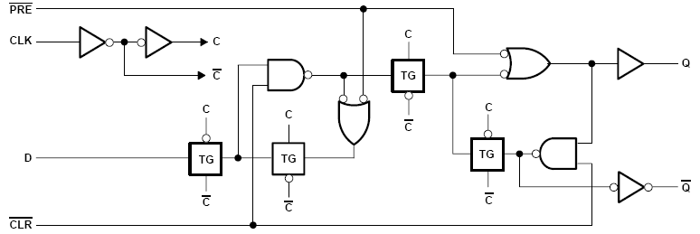
I am trying to understand the reset recovery and removal time in a flop architecture (made up of back to back inverters and transmission gates). Can anyone help me where and how to connect reset pin in a flop architecture?
Basically I am trying to compare with recovery/removal time with setup/hold time, and also want to understand why it is needed only during de-assertion of reset.

I am referring the following link to understand the setup/hold time
https://www.edn.com/design/analog/4371393/Understanding-the-basics-of-setup-and-hold-time


Regards,
Ashish
 

In the figure AND the Z signal of the master with the reset signal and then connect it to the transmission gate and in the same way do to the slave at the point P.
 

Hi Anand,
I think for the slave it should be OR of resetbar with point P.
 

Re: Warning for PRIYADHARSHINI PALANISAMY: Wrong Section

See the 74HC14 datsheet circuit. Essentially the inverters of the basic FF are replaced by NAND and NOR gates.

 
Hello Ashish,
For the Set signal you should have used a OR because when a set signal is set high the output should be always 1.If set and Reset are active low signals then use NOR and NAND respectively.Usually all the ICs which we see will be active low Reset and SET.So as FvM has said the above ckt can be used.
 

Re: Warning for PRIYADHARSHINI PALANISAMY: Wrong Section

Hi FvM,
By looking at this circuit, can I say that (assuming PRE is not active)

Required Recovery time for CLR = Delay of first NAND gate + Delay of first OR gate
Required Removal time for CLR = Switch OFF delay of Last TG - Delay of second NAND gate
 

Status
Not open for further replies.

Part and Inventory Search

Welcome to EDABoard.com

Sponsor

Back
Top