Continue to Site

Welcome to EDAboard.com

Welcome to our site! EDAboard.com is an international Electronics Discussion Forum focused on EDA software, circuits, schematics, books, theory, papers, asic, pld, 8051, DSP, Network, RF, Analog Design, PCB, Service Manuals... and a whole lot more! To participate you need to register. Registration is free. Click here to register now.

Step in microstrip lines

Status
Not open for further replies.

GIGER

Junior Member level 1
Joined
Mar 13, 2015
Messages
17
Helped
0
Reputation
0
Reaction score
0
Trophy points
1
Activity points
130
Hello guys.

I have a problem.
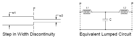
I'm designing a microstrip line and I have to put a step between two different lines as you can see in the uploaded figure.
Microstrip step.png

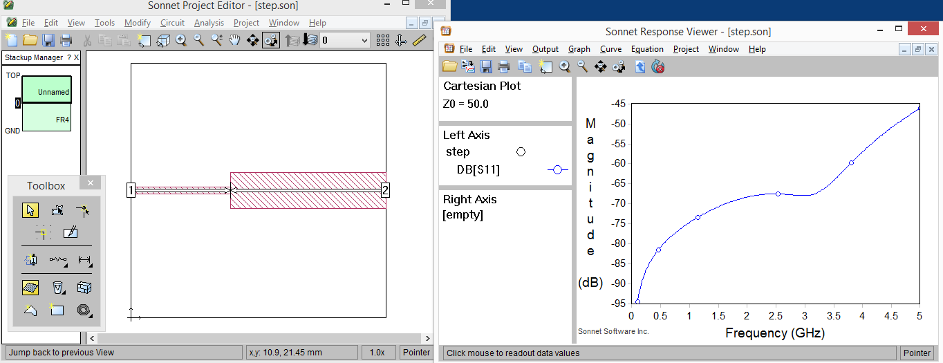
The simulated results are not any good and i want to ask if anyone knows a solution to this problem. Possibly a cut or whatever.

Thank you very much!
 

In Step Width Junction discontinuities the effect of the fringing capacitance associated with the wider line of the step discontinuity is similar to an increase in the length of that line.
The discontinuity capacitance C that appears due to the discontinuity has the effect of an increase in length of the wide line (2.8mm in your case), and an equal decrease in length of the narrow line (0.5mm).
To compensate for the excess capacitance, can make the wider line (2.8mm) to have the optimum electrically length. This length can be optimized by the simulator.


- - - Updated - - -

Also for discontinuity compensation you can add a taper.

http://cp.literature.agilent.com/litweb/pdf/ads2008/ccdist/3120823/ccdist-03-46-158.gif
 

The simulated results are not any good

What does "not good" mean?

Not what you expected or wanted?
Not correct for this layout?
How did you simulate and what data do you compared to?
 

Not good means the s11 is -15 - -20dB at my operating frequency.
I want it to be at least -30dB - -35dB.
I simulated the picture that i uploaded in my first post, fr4 substrate(er = 4.6, tand=0.018) and PEC on the bottom side(same dimensions as the fr4).
I want to minimize the parasitic capacitance that appears because of the step.

After some simulations i saw the following:
If I increase the length of the wider microstrip it appears different resonance frequencies. Nevertheless , the max value of S11 is at -15 - -20 dB too(at these frequencies).
So I want something to fix the step.
However, i tried a taper with a length 0.5mm connecting the two microstrips and the S11 was -25dB. My problem here is the length 0.5mm. I dont want it so small and if I increase its length, S11 is getting worse.
 

Not good means the s11 is -15 - -20dB at my operating frequency.
I want it to be at least -30dB - -35dB.

???

Any step in width is a discontinuity, and vfone showed the corresponding electrical model. Simulated alone, with no other objects, you will never see good return loss.

If I increase the length of the wider microstrip it appears different resonance frequencies. Nevertheless , the max value of S11 is at -15 - -20 dB too(at these frequencies).
So I want something to fix the step.

Now you talk about the line, not the step. Results for cascading different lines with different impedances is a different topic from "step in width", because this now includes the impedance transformation from the line length.

It is no clear what you are trying to do.
 

I just want -30dB or less S11 between port 1 and port 2. Nothing more nothing less.
The main problem here is the step, i didnt say the opposite. I'm trying to MINIMIZE the parasitic capacitance caused by the step. Any suggestions?
Cascading different lines is the same as step in width because the impedance microstrip transmition line is a function of its width. What do you mean?
 

It's still mysterious what you want to achieve. You are connecting MS lines of quite different impedance (at least 2:1 Z0 ratio) and get the respective reflection factor at the discontinuity (the s11 shoudn't be better than about -10 dB). To get rid of the signal reflection you need an impedance matching element. For small bandwidths, this can be a λ/4 transmission line segment.
 

I just want -30dB or less S11 between port 1 and port 2. Nothing more nothing less.

Including the lines on both sides, or just for the step itself (no length)?

Cascading different lines is the same as step in width because the impedance microstrip transmition line is a function of its width.

I disagree. The effect of the step (as calculated for example by **broken link removed**) is small compared to the effect of feedline impedance transformation.

- - - Updated - - -

This is what I get for your step geometry (step itself, excluding the line length on both sides): S11 better than -45dB up to 5GHz.


If you see a result that is worse, that is from the line impedance transformation of the non-50 Ohm line, not from parasitic capacitance of the step. Equivalent circuit model of the step extracted from S-parameters: 44fF shunt capacitance to ground, 75pH series inductance.
 
Last edited by a moderator:

Status
Not open for further replies.

Part and Inventory Search

Welcome to EDABoard.com

Sponsor

Back
Top