Continue to Site

Welcome to EDAboard.com

Welcome to our site! EDAboard.com is an international Electronics Discussion Forum focused on EDA software, circuits, schematics, books, theory, papers, asic, pld, 8051, DSP, Network, RF, Analog Design, PCB, Service Manuals... and a whole lot more! To participate you need to register. Registration is free. Click here to register now.

PVQFN footprint Making in ARES Guidance.

Status
Not open for further replies.

aliraza786

Full Member level 4
Joined
Nov 10, 2009
Messages
210
Helped
14
Reputation
28
Reaction score
14
Trophy points
1,298
Location
Lahore, Pakistan, Pakistan
Activity points
2,914
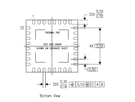
Hello Dear Members, i have to make pcb package of PVQFN package, i have the mechanical data of the footprint but there are 2 reading for each measurement i need to know which one is correct ? kindly guide me thanks.
 

Firstly look at and learn about IPC7351, secondly look for and learn about dimension basics, I would consider this a basic requirement for any one involved with any form of mechanical design process....
And yes PCB design is a mechanical design process, with tolerances base dimensions etc.
 

Status
Not open for further replies.

Part and Inventory Search

Welcome to EDABoard.com

Sponsor

Back
Top