Continue to Site

Welcome to EDAboard.com

Welcome to our site! EDAboard.com is an international Electronics Discussion Forum focused on EDA software, circuits, schematics, books, theory, papers, asic, pld, 8051, DSP, Network, RF, Analog Design, PCB, Service Manuals... and a whole lot more! To participate you need to register. Registration is free. Click here to register now.

Please let me know your idea about this circuit

Status
Not open for further replies.

MISU.RSG

Member level 1
Joined
Apr 29, 2011
Messages
34
Helped
2
Reputation
4
Reaction score
2
Trophy points
1,288
Activity points
1,581
Hi every body.
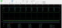
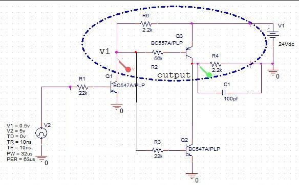
dears I want to make a circuit that its input is TTL and its output alternate between zero and 24V. I make one but it doesn't work properly .
I attached it and its wave form. green wave is for V1 and blue is output(Q3's voltage ).
please analyze it and let me know my mistake. I start to change the circuit but I like know why this circuit doesn't work. because I reach to desire wave form in simulation with orcad.
and if you have better idea let me be aware your idea.


56K at the base of Q3 slows down the switch off time. Try changing R6 and R2 to 4.7K .
It will be even better if you remove R6, change R2 to 2.2K and add 470R between base to emitter of Q3.
 

but it didn't come out very well
A kind of understatement as Q2 output has wrong polarity to support the output signal. There must be another inverting stage to implement a complementary output.
 

A kind of understatement as Q2 output has wrong polarity to support the output signal. There must be another inverting stage to implement a complementary output.
I've attached the corrected circuit to what I think the intention was. The problem with it is that it's a dangerous circuit that can draw too much current while switching.
It is better to have the circuit as it is and Q2 job will be to balance the PCB :)

 
Last edited:

In the corrected circuit, Q3 won't be turned off anymore with 24 V supply. R3 or R6 value must be adjusted to fix the problem. But basically a good option.
 

If R3 is changed to 56K and R6 to 1K you would probably accept it because Q2 and Q3 would switch on and off.
If the gain of the transistors is about 500 then when the input is about 1.2V the current through Q2 and Q3 will be about 1A, will you still call it a good option?
Good option should have both transistors as emitter followers.
 

Yeah. I think Vbase has the correct circuit for your intentions. I think you may be trying to build a magnetostriction circuit. You can tell from the reconfigure circuit if you try it.
 

Status
Not open for further replies.

Similar threads

Part and Inventory Search

Welcome to EDABoard.com

Sponsor

Back
Top