IntuitiveAnalog
Member level 2
Hi Everyone,
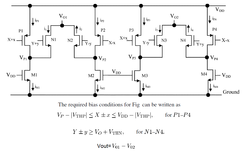
I am designing a multiplier circuit which has to act as a voltage squarer with Vout = (Vin^2)/25. The input waveform is sinusoidal with zero dc level ,100 mV peak to peak voltage and 10 kHz frequency.
I am having problem in adjusting biasing of the circuit .
I will be thankful if anybody can help.
--------------------------
Thanks
I am designing a multiplier circuit which has to act as a voltage squarer with Vout = (Vin^2)/25. The input waveform is sinusoidal with zero dc level ,100 mV peak to peak voltage and 10 kHz frequency.
I am having problem in adjusting biasing of the circuit .
I will be thankful if anybody can help.
--------------------------
Code:
***Multiplier***
Vdd 100 0 1.5
*.option scale=1u
.option post
.probe
.tran 0.1u 600u


Vp1 1 0 SIN(0.8V 0.2V 10k 0 0 0)
Vp2 7 0 SIN(0.8V 0.2V 10k 0 0 180)
Vp3 8 0 SIN(0.8V 0.2V 10k 0 0 0)
Vp4 12 0 SIN(0.8V 0.2V 10k 0 0 180)
Vn1 3 0 SIN(1.5V 0.1V 10k 0 0 0)
Vn2 5 0 SIN(1.5V 0.1V 10k 0 0 180)
Vn3 13 0 SIN(1.5V 0.1V 10k 0 0 180)
Vn4 14 0 SIN(1.5V 0.1V 10k 0 0 0)
Mp1 2 1 100 100 pmos W=0.8u L=0.35u
Mp2 6 7 100 100 pmos W=0.8u L=0.35u
Mp3 9 8 100 100 pmos W=0.8u L=0.35u
Mp4 11 12 100 100 pmos W=0.8u L=0.35u
Mn1 4 3 2 0 nmos W=0.8u L=0.35u
Mn2 4 5 6 0 nmos W=0.8u L=0.35u
Mn3 10 13 9 0 nmos W=0.8u L=0.35u
Mn4 10 14 11 0 nmos W=0.8u L=0.35u
M1 2 100 0 0 nmos W=0.8 L=0.35
M2 6 100 0 0 nmos W=0.8u L=0.35u
M3 9 100 0 0 nmos W=0.8u L=0.35u
M4 11 100 0 0 nmos W=0.8u L=0.35u

.MODEL nmos NMOS (                                LEVEL   = 49
+VERSION = 3.1            TNOM    = 27             TOX     = 7.7E-9
+XJ      = 1E-7           NCH     = 2.3579E17      VTH0    = 0.5048265
+K1      = 0.5542796      K2      = 0.0155863      K3      = 2.3475646
+K3B     = -3.3142916     W0      = 4.145888E-5    NLX     = 1.430868E-7
+DVT0W   = 0              DVT1W   = 0              DVT2W   = 0
+DVT0    = -0.0150839     DVT1    = 1.51022E-3     DVT2    = 0.170688
+U0      = 415.8570638    UA      = 5.057324E-11   UB      = 1.496793E-18
+UC      = 2.986268E-11   VSAT    = 1.237033E5     A0      = 0.9098788
+AGS     = 0.2120181      B0      = 1.683612E-6    B1      = 5E-6
+KETA    = -4.011887E-4   A1      = 0              A2      = 1
+RDSW    = 1.156967E3     PRWG    = -8.468558E-3   PRWB    = -7.678669E-3
+WR      = 1              WINT    = 5.621821E-8    LINT    = 1.606205E-8
+XL      = -2E-8          XW      = 0              DWG     = -6.450939E-9
+DWB     = 6.530228E-9    VOFF    = -0.1259348     NFACTOR = 0.3344887
+CIT     = 0              CDSC    = 1.527511E-3    CDSCD   = 0
+CDSCB   = 0              ETA0    = 1.21138E-3     ETAB    = -1.520242E-4
+DSUB    = 0.1259886      PCLM    = 0.8254768      PDIBLC1 = 0.4211084
+PDIBLC2 = 6.081164E-3    PDIBLCB = -5.865856E-6   DROUT   = 0.7022263
+PSCBE1  = 7.238634E9     PSCBE2  = 5E-10          PVAG    = 0.6261655
+DELTA   = 0.01           MOBMOD  = 1              PRT     = 0
+UTE     = -1.5           KT1     = -0.11          KT1L    = 0
+KT2     = 0.022          UA1     = 4.31E-9        UB1     = -7.61E-18
+UC1     = -5.6E-11       AT      = 3.3E4          WL      = 0
+WLN     = 1              WW      = -1.22182E-15   WWN     = 1.137
+WWL     = 0              LL      = 0              LLN     = 1
+LW      = 0              LWN     = 1              LWL     = 0
+CAPMOD  = 2              XPART   = 0.4            CGDO    = 3.5E-10
+CGSO    = 3.5E-10        CGBO    = 0              CJ      = 8.829973E-4
+PB      = 0.7946332      MJ      = 0.3539285      CJSW    = 2.992362E-10
+PBSW    = 0.9890846      MJSW    = 0.1871372      PVTH0   = -0.0148617
+PRDSW   = -114.7860236   PK2     = -5.151187E-3   WKETA   = 5.687313E-3
+LKETA   = -0.018518       )
*
.MODEL pmos PMOS (                                LEVEL   = 49
+VERSION = 3.1            TNOM    = 27             TOX     = 7.7E-9
+XJ      = 1E-7           NCH     = 8.52E16        VTH0    = -0.6897992
+K1      = 0.4134289      K2      = -5.342989E-3   K3      = 24.8361788
+K3B     = -1.4390847     W0      = 2.467689E-6    NLX     = 3.096223E-7
+DVT0W   = 0              DVT1W   = 0              DVT2W   = 0
+DVT0    = 1.3209807      DVT1    = 0.4695965      DVT2    = -8.790762E-4
+U0      = 150.6275733    UA      = 2.016943E-10   UB      = 1.714919E-18
+UC      = -1.36948E-11   VSAT    = 9.559222E4     A0      = 0.9871247
+AGS     = 0.3541967      B0      = 3.188091E-6    B1      = 5E-6
+KETA    = -0.0169877     A1      = 0              A2      = 1
+RDSW    = 2.443009E3     PRWG    = 0.0260616      PRWB    = 0.141561
+WR      = 1              WINT    = 5.038936E-8    LINT    = 1.650588E-9
+XL      = -2E-8          XW      = 0              DWG     = -1.535456E-8
+DWB     = 1.256904E-8    VOFF    = -0.15          NFACTOR = 1.5460516
+CIT     = 0              CDSC    = 1.413317E-4    CDSCD   = 0
+CDSCB   = 0              ETA0    = 0.3751392      ETAB    = 2.343374E-3
+DSUB    = 0.8877574      PCLM    = 5.8638076      PDIBLC1 = 1.05224E-3
+PDIBLC2 = 3.481753E-5    PDIBLCB = 2.37525E-3     DROUT   = 0.0277454
+PSCBE1  = 3.013379E10    PSCBE2  = 3.608179E-8    PVAG    = 3.9564294
+DELTA   = 0.01           MOBMOD  = 1              PRT     = 0
+UTE     = -1.5           KT1     = -0.11          KT1L    = 0
+KT2     = 0.022          UA1     = 4.31E-9        UB1     = -7.61E-18
+UC1     = -5.6E-11       AT      = 3.3E4          WL      = 0
+WLN     = 1              WW      = -5.22182E-16   WWN     = 1.125
+WWL     = 0              LL      = 0              LLN     = 1
+LW      = 0              LWN     = 1              LWL     = 0
+CAPMOD  = 2              XPART   = 0.4            CGDO    = 3.02E-10
+CGSO    = 3.02E-10       CGBO    = 0              CJ      = 1.397645E-3
+PB      = 0.99           MJ      = 0.5574537      CJSW    = 3.665392E-10
+PBSW    = 0.99           MJSW    = 0.3399328      PVTH0   = 0.0114364
+PRDSW   = 52.7951169     PK2     = 9.714153E-4    WKETA   = 0.0109418
+LKETA   = 7.702974E-3     )

.END
Thanks
Last edited by a moderator: