Continue to Site

Welcome to EDAboard.com

Welcome to our site! EDAboard.com is an international Electronics Discussion Forum focused on EDA software, circuits, schematics, books, theory, papers, asic, pld, 8051, DSP, Network, RF, Analog Design, PCB, Service Manuals... and a whole lot more! To participate you need to register. Registration is free. Click here to register now.

ADCPARALLEL-de1soc_FPGA-dacSPI

Status
Not open for further replies.

jimmykk

Full Member level 3
Joined
Oct 2, 2014
Messages
158
Helped
0
Reputation
0
Reaction score
1
Trophy points
1,298
Activity points
2,863
Hi
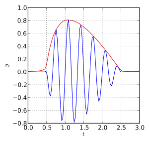
I have a problem getting output from DAC AD5641(14-BIT). Input first goes from adc(LTC2245) to Fpga and negative cycle gets removed and output should come from dac. Input is .5V 200khz , clock 5mhz. can someone tell me where am i doing wrong. Output should be only a pos cycle of input.
Thanks


Code VHDL - [expand]
1
2
3
4
5
6
7
8
9
10
11
12
13
14
15
16
17
18
19
20
21
22
23
24
25
26
27
28
29
30
31
32
33
34
35
36
37
38
39
40
41
42
43
44
45
46
47
48
49
50
51
52
53
54
55
56
57
58
59
60
61
62
63
64
65
66
67
68
69
70
71
72
73
74
75
76
77
78
79
80
81
82
83
84
85
86
87
88
89
90
91
92
93
94
95
96
97
98
99
100
101
102
103
104
105
106
107
108
109
110
111
112
113
114
115
116
117
118
119
120
121
122
123
124
125
126
127
128
129
130
131
132
133
134
135
library ieee;
use ieee.std_logic_1164.all;
 
use ieee.numeric_std.all;
 
 
entity ADC_PARALLEL is
port(
clock_50  : in std_logic;
LEDR      : out std_logic_vector(9 downto 0);
GPIO_1    : inout std_logic_vector(35 downto 0)
 
 
);
end ADC_PARALLEL;
 
architecture arch of ADC_PARALLEL is
type state_type is (IDLE,READ_DATA,WAIT_STATE,WRITE_DATA);
signal state  : state_type := IDLE;                  --initial state
 
 
signal clk_div : integer range 0 to 5 := 0;
signal clock_5 : std_logic := '0';
signal adc_data : std_logic_vector(13 downto 0) := "00000000000000";
signal positiv_cycle : unsigned(12 downto 0);             -- positive cycle data from adc 
signal count   : integer range 0 to 16 := 0;


begin
GPIO_1(6) <= '0';                 -- SHDN TO GROUND, SHOULD BE GROUND FOR NORMAL OPERATION OF ADC
GPIO_1(1)  <= clock_5;            -- 5MHZ OUT
GPIO_1(30) <= clock_5;            -- 5MHZ OUT
               
process(clock_50)      -- CLOCK DIVISION PROCESS
begin
if(rising_edge(clock_50)) then
if (clk_div = 4) then
clock_5 <= clock_5 xor '1';
clk_div <= 0;
else  
clk_div <= clk_div + 1;
end if;
end if;
end process;
 
 
process(clock_5)              --MAIN PROCESS
 
begin
if (rising_edge(clock_5)) then


--if(clk_div  = 4 and clock_5 = '0') then      -- DATA CHANGED ON RISING EDGE OF CLOCK
case state is
 
 
when IDLE =>
GPIO_1(0) <= '1';           -- DAC SYNC HIGH, DAC NOT IN WRITE MODE
GPIO_1(2) <= '0';           -- DAC SERIAL DATA OUT 
GPIO_1(7) <= '1';           -- OE high, adc disabled
positiv_cycle <= (others => '0');
if (count = 16) then
count <= 0;
state <= READ_DATA;
else 
count <= count + 1;
state <= IDLE;
end if;
 
when READ_DATA =>                     --  FOR one clock cycle
GPIO_1(0) <= '1';                     --  dac sync high, no write
GPIO_1(7) <= '0';                     -- OE down to 0,adc enabled, NORMAL OPERATION
GPIO_1(31) <= '0';                    -- OF BIT of ADC disabled, coz input is max. 500mVpp
--positiv_cycle <= "0000000000000";
adc_data(13 downto 0) <= GPIO_1(25 downto 12); -- INPUT FROM GPIO BUS, 14 BITS COMING
LEDR(8 downto 0)     <= GPIO_1(25 downto 17);
if(count = 0) then
count <= count + 1;
state <= READ_DATA;
elsif(count = 1) then
if adc_data(13) = '1' then            -- check MSB, IF '1' then positive cycle of wave OFFSET BINARY OUTPUT FORMAT
positiv_cycle <= unsigned(adc_data(12 downto 0));
--LEDR(9 downto 1) <= std_logic_vector(positiv_cycle(12 downto 4));
count <= 0;
state <= WAIT_STATE;
else                                  -- ELSE FOR NEGATIVE CYCLE, ALL BITS = 0
positiv_cycle <= "0000000000000";
--LEDR(9 downto 1) <= std_logic_vector(positiv_cycle(12 downto 4));
count <= 0;
state <= WAIT_STATE;
end if;
end if;
 
when WAIT_STATE =>
GPIO_1(0) <= '1';               -- sync high
GPIO_1(7) <= '1';               -- OE BACK HIGH OF ADC LTC2245
count <= 0;
--adc_data <= "00000000000000";
state <= WRITE_DATA;
 
 
when WRITE_DATA =>
GPIO_1(0) <= '0';
GPIO_1(7) <= '1';
LEDR <= (others => '0');
if(count = 0 or count = 1) then     -- NORMAL WRITE OOPERATION OF DAC-SPI, FIRST TWO BITS SHOULD BE 0
GPIO_1(2) <= '0';
count <= count+1;
state <= WRITE_DATA;
elsif(count = 2) then               -- HAS TO BE 0 BECAUSE ONLY 13 BITS ARE TO BE TRANSFERRED
GPIO_1(2) <= '0';
count <= count + 1;
state <= WRITE_DATA;
elsif(count > 2 and count < 16) then -- 13 BITS TRANSFEREED SERIALLY
GPIO_1(2) <= std_logic(positiv_cycle(15 - count));
count <= count + 1;
state <= WRITE_DATA;
 
elsif (count = 16) then
GPIO_1(0) <= '1';
GPIO_1(2) <= '0';
count <= 0;
state <= READ_DATA;
end if;


end case;
end if;
--end if;
end process;
 
end architecture;

 
Last edited by a moderator:

1. I didn't try to simulate your code for functional correctness - but at first glimpse, I can see bad design practices implemented in it:
For example: the usage of the "clock_5" signal.
Not saying that this is the source of your problem. Just a general note.

2. Are you sure that the source of your problem is the block that controls the ADC ?

Post all of your code - including the test bench files that you used to verify your design with.
 

Thanks for response....i know that i should have used the system clock instead of clock_5, but it is not creating any problem. My eventual goal is to get an envelope of the positive cycle by taking the abs value.
I am thinking of replacing the operation In READ_DATA state to
positiv_cycle <= std_logic_vector(abs(signed(adc_data(13 downto 0))));
and then passing this positiv_cycle to GPIO_1(2)(OR Din of DAC)

- - - Updated - - -


http://obrazki.elektroda.pl/6005911500_1429362838.png
 

Post your full code + test bench
 

Thanks for response....i know that i should have used the system clock instead of clock_5, but it is not creating any problem.

It may not be causing you a problem now, but quite easily cause a problem the next time you compile the code. Or when your chip gets hot. Or when you put it in another chip.

I highly recommend you switch to the system clock now, as it could cause you a problem without warning.
 

Status
Not open for further replies.

Part and Inventory Search

Welcome to EDABoard.com

Sponsor

Back
Top