Continue to Site

Welcome to EDAboard.com

Welcome to our site! EDAboard.com is an international Electronics Discussion Forum focused on EDA software, circuits, schematics, books, theory, papers, asic, pld, 8051, DSP, Network, RF, Analog Design, PCB, Service Manuals... and a whole lot more! To participate you need to register. Registration is free. Click here to register now.

Charge pump design problem

Status
Not open for further replies.

EHY

Member level 1
Joined
Apr 2, 2015
Messages
36
Helped
0
Reputation
0
Reaction score
0
Trophy points
6
Activity points
235
CP.PNG
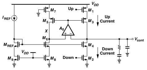
I designed Charge pump like attached image.

When UP signal is turn on (width 100ps) current of pink color node switching quite properly.

but problem is that mirroring current of UP current(blue color node) is not fast switching.

so how can i increase switching speed of bule color node current??

i want to increase length of MOSFET to decrease UP/DN current mismatch.
 

Maybe the frequency at which you are switching the pink color current is close to the -3 dB cut-off frequency of the mirrored pmos transistor (right side up) together with the driver nmos transistor having input DN.
Maybe due to the large output resistance of that pmos transistor, it is having a smaller bandwidth. I think if you increase the W/L ratios of all the transistors proportionately by keeping them in saturation a larger current will flow through them leading to smaller output resistance of the pmos transistor (1/λID).
But I cant tell what your power budget is?
 

Charge pump circuit is designed on 180nm CMOS technology.

and width of UP, DN pulse is 100ps (In CDR circuit 5Gb/s(1UI=200ps), lock condition UP=0.5UI DN:0.5UI (full rate hogge PD))

is it impossible on 180nm technology(speed limitation)???


Maybe the frequency at which you are switching the pink color current is close to the -3 dB cut-off frequency of the mirrored pmos transistor (right side up) together with the driver nmos transistor having input DN.
Maybe due to the large output resistance of that pmos transistor, it is having a smaller bandwidth. I think if you increase the W/L ratios of all the transistors proportionately by keeping them in saturation a larger current will flow through them leading to smaller output resistance of the pmos transistor (1/λID).
But I cant tell what your power budget is?
 

The cut-off frequency of a simple inverter in UMC 180nm technology biased in saturation region can be up to 2 GHz. You can reach higher frequencies like 2.4 GHz in 180nm by using inductors as loads. One such example is RF Low Noise Amplifiers. Your operating frequency is 5 GHz.

The pmos transistor in the upper right corner of the circuit is acting as a current-source load and has a high output resistance. Maybe its bandwidth cannot be more than 500 MHz.
My opinion is you can either use inductors in your design or maybe go to lower technology nodes like 90nm...

However that is my opinion!! I may be wrong. Maybe you should wait for any other responses to this topic!!
 

Thank you your opinion.

i have one question.

how can i test my CMOS technology cut off frequency??(speed limit) in cadence


The cut-off frequency of a simple inverter in UMC 180nm technology biased in saturation region can be up to 2 GHz. You can reach higher frequencies like 2.4 GHz in 180nm by using inductors as loads. One such example is RF Low Noise Amplifiers. Your operating frequency is 5 GHz.

The pmos transistor in the upper right corner of the circuit is acting as a current-source load and has a high output resistance. Maybe its bandwidth cannot be more than 500 MHz.
My opinion is you can either use inductors in your design or maybe go to lower technology nodes like 90nm...

However that is my opinion!! I may be wrong. Maybe you should wait for any other responses to this topic!!
 

Suppose you want to want to find out the bandwidth of a CS amplifier with resistive load.
Set a nmos transistor with W/L=2u/1u. Add a load resistance of 1K. Now vary the gate voltage of the nmos from 0 to Vdd. Plot the output voltage. You'll get a curve similar to an inverter transfer characteristics.
Generally we want to set the bias point for an amplifier for maximum gain. So you can take the derivative of the output voltage curve and find out the input voltage for maximum value of the derivative (derivative of Vout vs Vin = Gain of the amplifier).
Now add a dc voltage to the input whose dc magnitude is the value of input voltage for maximum gain. Add ac magnitude = 1V.
Now do the ac analysis, vary the frequency from 1K to 100G.
Go to results -> direct plot -> ac dB20 -> select the output node and escape.
You'll get the gain magnitude plot in dB scale. Suppose the gain at 1K is 18 dB. Then the cut-off frequency or 3 dB bandwidth will be the frequency where the gain falls to (18-3)=15 dB.

I hope this helped.
 

how can i test my CMOS technology cut off frequency??(speed limit) in cadence

Instead of your transient simulation, run an ac analysis and plot the resulting voltage (at any node of interest) vs. frequency. The -3dB decline point is the cut off frequency.

Note: This is schematic. In layout you'll have additional parasitic capacitances, which may considerably decrease this cut off frequency.
 

Then, how can I test the maximum speed(BW)of charge pump I attached above??

In case of CS amp, I understood your advice.


Suppose you want to want to find out the bandwidth of a CS amplifier with resistive load.
Set a nmos transistor with W/L=2u/1u. Add a load resistance of 1K. Now vary the gate voltage of the nmos from 0 to Vdd. Plot the output voltage. You'll get a curve similar to an inverter transfer characteristics.
Generally we want to set the bias point for an amplifier for maximum gain. So you can take the derivative of the output voltage curve and find out the input voltage for maximum value of the derivative (derivative of Vout vs Vin = Gain of the amplifier).
Now add a dc voltage to the input whose dc magnitude is the value of input voltage for maximum gain. Add ac magnitude = 1V.
Now do the ac analysis, vary the frequency from 1K to 100G.
Go to results -> direct plot -> ac dB20 -> select the output node and escape.
You'll get the gain magnitude plot in dB scale. Suppose the gain at 1K is 18 dB. Then the cut-off frequency or 3 dB bandwidth will be the frequency where the gain falls to (18-3)=15 dB.

I hope this helped.
 

I guess the average voltage for UP signal is 1.3 V. So add a dc source whose dc magnitude is 1.3 V and ac magnitude 1 V.
Then do the ac analysis. Vary the frequency from 1K to 100G. Plot the ac dB20 of drain voltage of the upper right pmos transistor.
If it dosen't show anything, then maybe you have to disconnect the voltage source that have been connected at the output node.
Then do the analysis once again.
 

oh thank you so much

i have last one question

do you think that other topology of charge pump except gate switching charge pump will not switch fastly like the attached image due to 180nm technology speed limit??!


I guess the average voltage for UP signal is 1.3 V. So add a dc source whose dc magnitude is 1.3 V and ac magnitude 1 V.
Then do the ac analysis. Vary the frequency from 1K to 100G. Plot the ac dB20 of drain voltage of the upper right pmos transistor.
If it dosen't show anything, then maybe you have to disconnect the voltage source that have been connected at the output node.
Then do the analysis once again.
 

I dont have much knowledge about charge pump. Once I used it in a PLL circuit. It had an upper pmos current source with an UP switch and a lower nmos sink with a DN switch. The outout load was a capacitance resistance loop filter.
That circuit worked fine in 400 MHz. You can search for it in the net as PLL Charge Pumps.
 

bw.PNG

as you mentioned above, i did AC analysis like attacehd image.

so in this graph, BW of upper right pmos is 205.4MHz?

I guess the average voltage for UP signal is 1.3 V. So add a dc source whose dc magnitude is 1.3 V and ac magnitude 1 V.
Then do the ac analysis. Vary the frequency from 1K to 100G. Plot the ac dB20 of drain voltage of the upper right pmos transistor.
If it dosen't show anything, then maybe you have to disconnect the voltage source that have been connected at the output node.
Then do the analysis once again.
 

No, this is not the correct graph!!
Some of the transistors may not be in saturation region, they might be in linear region.
Give 1.3V in the UP signal. Give appropriate dc voltage to DN signal. Do dc analysis. See if all the transistors are in saturation.
Note that the transistors should show "region 2" after dc analysis if they are in saturation.
 

Thank you for your kindness.

i have solved the speed limit problem by using a differential output current topology (attached image)

but i have problem. My CMOS technology does not support RF element(inductor)

i can not design LC VCO

because of differetial output current of Charge pump, i need differential Loop fillter and i have to convert differential control voltage to single-ended control voltage.

so differetial to single converter must have high bandwidth to convert the differetial control voltage that switches fast.

i am worried that it is difficult to make differential input to single-ended ouput amp(converter) that has 5GHz bandwidth in 180nm technology.

do you happen to know differentially tuned ring type VCO??

i am sorry to bother you. :oops:solution.PNG


No, this is not the correct graph!!
Some of the transistors may not be in saturation region, they might be in linear region.
Give 1.3V in the UP signal. Give appropriate dc voltage to DN signal. Do dc analysis. See if all the transistors are in saturation.
Note that the transistors should show "region 2" after dc analysis if they are in saturation.
 

Found a paper where they are using varactors and applying differential control voltage to the varactor network.

"A 38 GHz accumulation MOS differentially tuned VCO design in 0.18µm CMOS" - Carr, Frank
 

differential charge pump must have CMFB(common mode feedback) circuit ??


Found a paper where they are using varactors and applying differential control voltage to the varactor network.

"A 38 GHz accumulation MOS differentially tuned VCO design in 0.18µm CMOS" - Carr, Frank
 

The problem is like that in a two stage opamp or in cascoded opamp.
In two stage opamp the output stage has problem of current matching, so also in cascoded opamp where it is even more severe.
Generally in single-ended charge pump, a feedback can be provided like this to avoid the current mismatch problem.

This is from the book RF Microelectronics - Razavi.
You can also use cmfb to reduce the current mismatch between the UP and DN paths. It is in detail in Razavi's book (Analog CMOS Integrated Circuits)
 

Status
Not open for further replies.

Similar threads

Part and Inventory Search

Welcome to EDABoard.com

Sponsor

Back
Top