yolco
Member level 2
Hi,
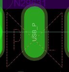
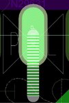
can someone explain me what is happening with PCB editor and this DRC Error, Line to SMD Pin Spacing (pictures attached)?
Explanation:
KR!
- - - Updated - - -
Forget it!
PCB Editor error, nothing related to PCB design.
can someone explain me what is happening with PCB editor and this DRC Error, Line to SMD Pin Spacing (pictures attached)?
Explanation:
- First, I route the USB_P trace, and no DRC error is shown.
- Then, I don't know how, the USB_P trace was hidden, but DRC error appears.

- Now, USB_P is hidden unless I mark the DRC error which shows de Cline seg.

- I can't select the hidden trace, nor remove it, neither do anything with it. But DRC error still persists.
KR!
- - - Updated - - -
Forget it!
PCB Editor error, nothing related to PCB design.