IntuitiveAnalog
Member level 2
Hi All,
I am designing a two stage miller opamp (pmos input differential pair) in subthreshold region. I am using 32nm technology node. The parameters are given below:
1. Supply voltage = 1V
2. Bias Current = 200nA
3. Transistor Length = 160nm=(5 Lmin)
There are no specific requirements but I have to just reduce power dissipation.
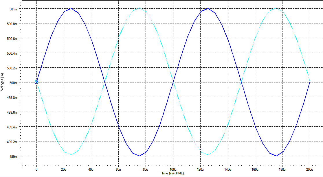
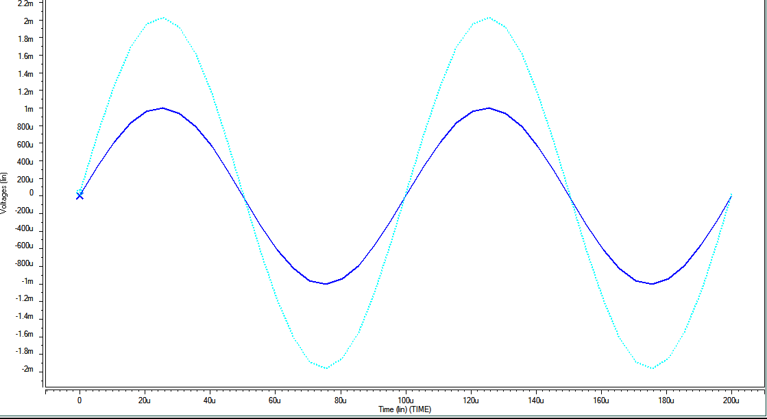
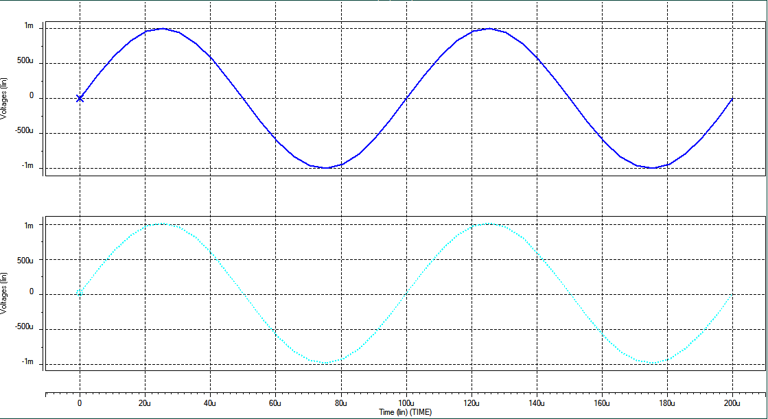
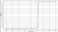
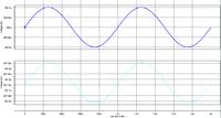
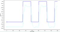
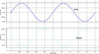
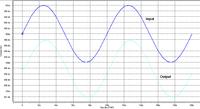
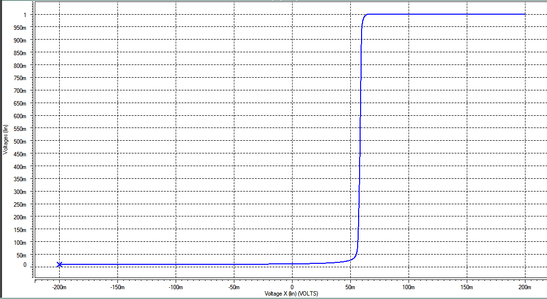
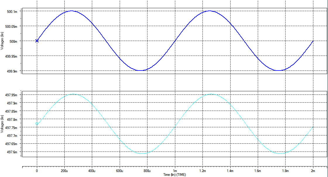
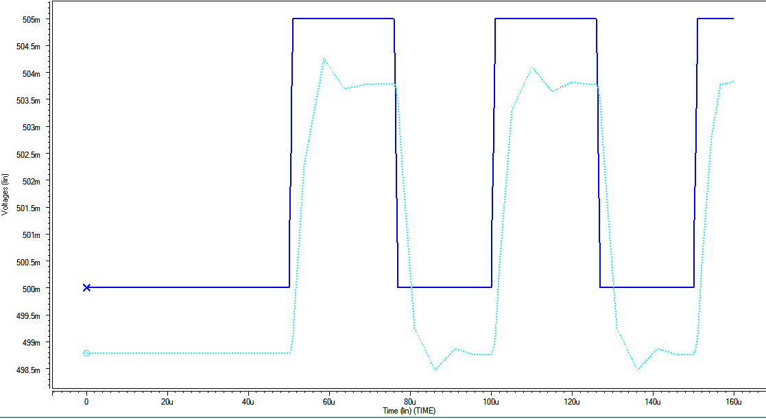
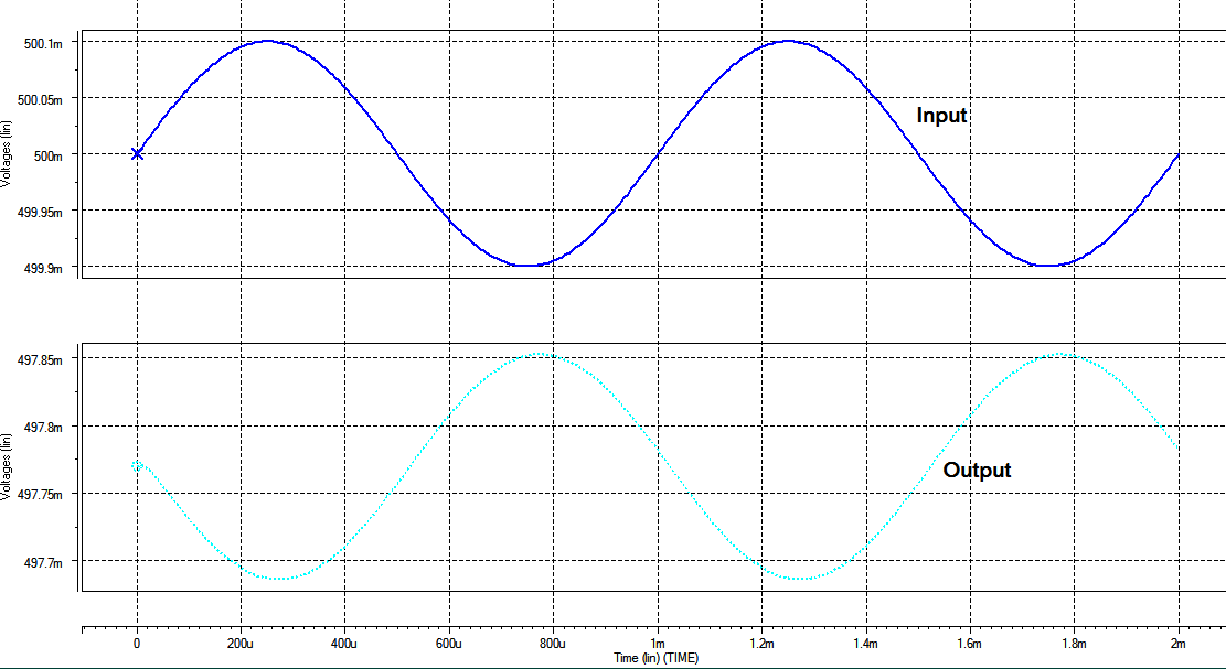
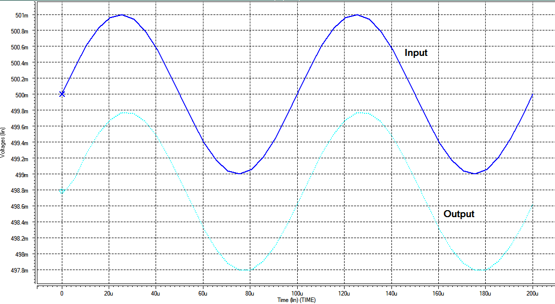
I am getting all the responses quite correct but in transient analysis the output dc level is not the same as input dc level.
I will be very much thankful if anyone could figure out how to make input and output dc level same.
Thanks
I am designing a two stage miller opamp (pmos input differential pair) in subthreshold region. I am using 32nm technology node. The parameters are given below:
1. Supply voltage = 1V
2. Bias Current = 200nA
3. Transistor Length = 160nm=(5 Lmin)
There are no specific requirements but I have to just reduce power dissipation.
I am getting all the responses quite correct but in transient analysis the output dc level is not the same as input dc level.
I will be very much thankful if anyone could figure out how to make input and output dc level same.

Thanks