Continue to Site

Welcome to EDAboard.com

Welcome to our site! EDAboard.com is an international Electronics Discussion Forum focused on EDA software, circuits, schematics, books, theory, papers, asic, pld, 8051, DSP, Network, RF, Analog Design, PCB, Service Manuals... and a whole lot more! To participate you need to register. Registration is free. Click here to register now.

[Moved]: Buck converter stability

Status
Not open for further replies.

kah89

Junior Member level 2
Joined
Feb 9, 2015
Messages
24
Helped
0
Reputation
0
Reaction score
0
Trophy points
1
Activity points
169
Hi,

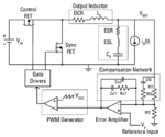
I have a question about the stability analysis of the Buck converter

the circuit of buck is a combination between analog and digital how to model the digital circuits to make the stability and loop analysis

Thanks in advance
 

Re: Buck converter stability

Hi

From my experience it is a though job to do stb analysis (ac-based analysis) on a whole buck DC-DC system, because it is a complex system with PWM involved.

What you can do, and is usually done, is model all your analog components (opa, comparator, reference) on stand-alone, and then design your feedback network based on your input specifications.

For system -or top-level simulations- of your whole buck, you should do all kind of transient simulations, and check for proper behavior of your DC-DC
 
  • Like
Reactions: kah89

    kah89

    Points: 2
    Helpful Answer Positive Rating
You can model everything as linear blocks to perform an AC (small signal) stability analysis (either by calculation or simulation).
For example, the PWM part of the circuit converts the error voltage to a PWM duty-cycle which generates a voltage at the converter output as determined by the input voltage and the duty-cycle. So you calculate what the transfer function gain is from the error voltage to the output voltage. This then becomes a linear block in the circuit for the AC analysis.

Thus, suppose a 0V error signal generates a 0% duty-cycle and a 2V error signal generates a 100% duty-cycle, and the supply voltage is 15V. Then the transfer gain of this circuit is 15V/2V =7.5 (since the average output voltage of an ideal PWM is a linear function of duty-cycle with 0V at 0% duty-cycle and equal to the supply voltage at 100% duty-cycle).

Determining this transfer function with an IC PWM modulator chip can require some digging. For one chip I used I had to look at the internal block diagram and the listed parameters for some functions, such as the sawtooth amplitude used to generate the PWM signal along with the internal error amplifier gain, to calculate the transfer function.
 
Last edited:
  • Like
Reactions: kah89

    kah89

    Points: 2
    Helpful Answer Positive Rating
You can model everything as linear blocks to perform an AC (small signal) stability analysis (either by calculation or simulation).
For example, the PWM part of the circuit converts the error voltage to a PWM duty-cycle which generates a voltage at the converter output as determined by the input voltage and the duty-cycle. So you calculate what the transfer function gain is from the error voltage to the output voltage. This then becomes a linear block in the circuit for the AC analysis.

Thus, suppose a 0V error signal generates a 0% duty-cycle and a 2V error signal generates a 100% duty-cycle, and the supply voltage is 15V. Then the transfer gain of this circuit is 15V/2V =7.5 (since the average output voltage of an ideal PWM is a linear function of duty-cycle with 0V at 0% duty-cycle and equal to the supply voltage at 100% duty-cycle).

Determining this transfer function with an IC PWM modulator chip can require some digging. For one chip I used I had to look at the internal block diagram and the listed parameters for some functions, such as the sawtooth amplitude used to generate the PWM signal along with the internal error amplifier gain, to calculate the transfer function.

Thank you so much, I really appreciate your answer.

If you don't mind I have another question. I am working now on the compensation circuit, I know from control theory that "type n system" means system which have n poles at the origin but in Buck "type 3" has only one pole at the origin? and that made me confused.
 

Hi again

For the type of compensation needed, this depends on the topology you choose for your buck converter.
Is it based on a voltage controlled or current controlled loop?
Based on this, you will need a compensation network with either 2 poles and to zeros, or 1 pole and 1 zero (respectively)
 
  • Like
Reactions: kah89

    kah89

    Points: 2
    Helpful Answer Positive Rating
Hi again

For the type of compensation needed, this depends on the topology you choose for your buck converter.
Is it based on a voltage controlled or current controlled loop?
Based on this, you will need a compensation network with either 2 poles and to zeros, or 1 pole and 1 zero (respectively)

Thank you, But when the compensator has 3 poles it is called type 3 compensator and I have read that type n system means system have n poles at the origin and type 3 compensator has only one pole at the origin.

P.S : I am using voltage controlled.
 

What is the effect of duty cycle on the stability of Buck converter?

What is the effect of duty cycle of the square wave output from the comparator on the stability of Buck converter?

c0799-figure1.gif
 
Last edited:

Depends on DCM or CCM operation. No effect in CCM (continuous mode), but duty cycle is changing the loop gain in DCM, calculate yourself.
 

Status
Not open for further replies.

Similar threads

Part and Inventory Search

Welcome to EDABoard.com

Sponsor

Back
Top