Continue to Site

Welcome to EDAboard.com

Welcome to our site! EDAboard.com is an international Electronics Discussion Forum focused on EDA software, circuits, schematics, books, theory, papers, asic, pld, 8051, DSP, Network, RF, Analog Design, PCB, Service Manuals... and a whole lot more! To participate you need to register. Registration is free. Click here to register now.

Errors in Layout versus Schematic(LVS) match of 6T SRAM

Status
Not open for further replies.

Hacralo

Newbie level 4
Joined
Feb 11, 2015
Messages
7
Helped
0
Reputation
0
Reaction score
0
Trophy points
1
Activity points
52
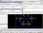
I am doing a LVS match of a 6T SRAM using 180nm technology. First I made a schematic of 6T SRAM and then generated the layout from schematic using Layout XL , and made some additional routings. i successfully ran the DRC. But while doing the LVS match I am getting the errors like one pin,device, parameter mismatch. It would be really appreciated if someone could check the layout and schematic images attached below and point out the errors i have commited. layout.pnglayout2.png
 

Perhaps you should show all your error messages.

BTW: Why do you use such asymmetric width values for NM0/1 and PM0/1 ? Preference for a certain logic value?
 

Here is error screenshot:Screenshot-2.png
 

I think these problems/warnings just arise from pin labels which overlap each other. Make them as small as the pins themselves. For your own orientation you could use additional text labels in the current size, which don't disturb the LVS.

Anyway: success.gif
 

Ok, I have made certain changes and now I am getting a parameter mismatch and net mismatch. In parameter mismatch, it says size of 4 transistors are different in schematic and layout, but I generated these transistor layouterror13.pnglayout111.pngpinparam.pngschematic12.pngs from schematic itself. And I am also getting 6 label shots
Here are some screenshots:
 

I can't find an error from your layout111, because there aren't any text labels. Did you try and check the warning coordinates notes and enter the LVS Debug Environment to get more help?

Meanwhile I assume you have too many pin labels in your layout which interact and entangle the LVS run. Count them by making just pin layer or pin label layer selectable (all other layers non selectable) and select all. If something's wrong, I'd suggest to remove all of them and add new correct pins & pin label names.

It is possible that the parameter mismatch error is just pretended by (possible) pin mismatches.
 

I rectified my mistakes and now am not getting any errors, thanks!
 

hi everyone. i have a similar problem

I made layouts in the cadence CDB (5.1.4.1) and i placed hundreds of labels with any problem. Now i'm trying a simple inverter in the version OA (6.1.3) but i found the next problems:
-the label option does not pop up any window
-I add then through the pin option, nevertheless, the text is not visible and i tried different font sizes. The corresponding metal polygon is in the layout
-I use vdda and vssa for vdd and gnd instead the global signals vdd! and gnd!. defining vdda and vssa as power pins in calibre it worked fine in the cdb version. in the OA i get the next errors:

Warning: #1 in inverter
WARNING: Invalid PATHCHK request "GROUND && ! POWER": no POWER nets present, operation aborted.

Warning: #2 in inverter
WARNING: Invalid PATHCHK request "POWER && ! GROUND": no POWER nets present, operation aborted.

Warning: #3 in inverter
WARNING: Invalid PATHCHK request "! LABELED": no LABELED nets present, operation aborted.

Warning: #4 in inverter
WARNING: Invalid PATHCHK request "! POWER && ! GROUND": no POWER nets present, operation aborted.
of course, the LVS brakes.
I guess that calibre does not detect the pins, the question is why? and other question: why the "create label" does not work?
did someone has the same problems and has found the solution?

Thank you very much in advance
 

Could be either the text is at the wrong level of hierarchy, or not referenced in the rules. See **broken link removed** for a more in-depth explanation and link to an app note.
 

Status
Not open for further replies.

Part and Inventory Search

Welcome to EDABoard.com

Sponsor

Back
Top