vdalegro
Newbie level 6
Hello,
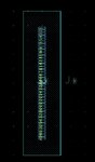
I create a connector FPC using Package symbol (wizard) de Allegro PCB editor but I got finally a symbol amazing (see photo attached). I don't see the pads properly in the symbol but I can see the pad in 3D. I have turned on all color layers.
Have you see the same problem ?
Thanks
I create a connector FPC using Package symbol (wizard) de Allegro PCB editor but I got finally a symbol amazing (see photo attached). I don't see the pads properly in the symbol but I can see the pad in 3D. I have turned on all color layers.
Have you see the same problem ?
Thanks