Welcome to our site! EDAboard.com is an international Electronics Discussion Forum focused on EDA software, circuits, schematics, books, theory, papers, asic, pld, 8051, DSP, Network, RF, Analog Design, PCB, Service Manuals... and a whole lot more! To participate you need to register. Registration is free. Click here to register now.
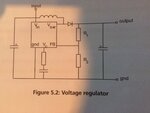
Vsw shorts the right side of the inductor to ground which charges up it's current. When Vsw opens, that current has to go somewhere (inductors resist instant current changes) and ends up pumping current through the diode into the output capacitor. This allows the boost converter to produce an output voltage higher than the input voltage.
The chip presumable has an internal reference and controlls the Vsw on time versus off time so as to regulate the FB pin to a certain voltage (like 0.6V). The resistor divider determines what voltage on the output creates 0.6V (for example) on the FB pin, thus setting the output voltage.
the higher the value of the upper resistor, the higher the output voltage, considering that you keep the lower one the same.
the diagram doesn't show the negative feedback loop that probably exists inside the controller.
Remember the law...opamp with negative feedback drives its output until its inputs are the same voltage.....there you have it.....if the ref is 0.6v, then make your voltage divider give 0.6v to the error amp input when your vout is your required voltage.
you asked what isinside it...search on google "linear.com micro boost controller"
-then you wuill find datasheet that tell you what is inside it...you can even simulate it with their free sim ltspice
This site uses cookies to help personalise content, tailor your experience and to keep you logged in if you register.
By continuing to use this site, you are consenting to our use of cookies.