Continue to Site

Welcome to EDAboard.com

Welcome to our site! EDAboard.com is an international Electronics Discussion Forum focused on EDA software, circuits, schematics, books, theory, papers, asic, pld, 8051, DSP, Network, RF, Analog Design, PCB, Service Manuals... and a whole lot more! To participate you need to register. Registration is free. Click here to register now.

Transistor based Buck converter help

Status
Not open for further replies.

mohsin_hashmi

Newbie level 2
Joined
Sep 11, 2012
Messages
2
Helped
0
Reputation
0
Reaction score
0
Trophy points
1,281
Activity points
1,295
Hi,

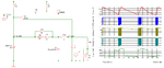
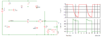
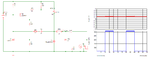
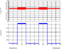
Can anyone please make me clear the purpose of
R3,R4 and C2 in this circuit. How this circuit actually works?

Thank You
Link: https://www.eleccircuit.com/12-volts-switching-power-supply-using-transistor/

12-volts-switching-power-supply-using-transistor-600x400.jpg
 

Yes that seems like it, but I am interested in this particular circuit. Any idea how R3,R4 and C2 function in this circuit.
 

That circuit acts to peak the leading edge of the switching signal to the T2 base. This apparently is to reduce the switching speed of T2 to improve efficiency.

But I see no advantage of that over the Roman Black design which uses just a capacitor.

Note that L1 is likely 220µH.
 

I have seen some variations of these. The one shown in the first post does seem to have some starting problems with lower loads and some other problems.

The "black" design works well when simulated with good efficiency (~90%) and good regulation.

The power FET version with a TL431 is an idea I played with before that gives better regulation and similar efficiency of just over 90% at 500 mA load. Even at 1 A load it looks good.
 

Attachments

  • buck_prob.png
    buck_prob.png
    36.3 KB · Views: 147
  • RB_500m12V.png
    RB_500m12V.png
    36.4 KB · Views: 154
  • FET_500m12V.png
    FET_500m12V.png
    30.6 KB · Views: 171
  • FET_1000m12V.png
    FET_1000m12V.png
    13.4 KB · Views: 118
Last edited:

I like the idea of the TL431 as a reference in place of the zener.
That provides regulation directly at the output and allows for an adjustable voltage by varying the ratio of R4 to R5.
 

I did this design to serve as a very efficient tracking pre-regulator for a lab power supply.
 

Status
Not open for further replies.

Similar threads

Part and Inventory Search

Welcome to EDABoard.com

Sponsor

Back
Top