Continue to Site

Welcome to EDAboard.com

Welcome to our site! EDAboard.com is an international Electronics Discussion Forum focused on EDA software, circuits, schematics, books, theory, papers, asic, pld, 8051, DSP, Network, RF, Analog Design, PCB, Service Manuals... and a whole lot more! To participate you need to register. Registration is free. Click here to register now.

Analog passive filter design for Complex load(inductive and capacitive)

Status
Not open for further replies.

chandresha1

Member level 2
Joined
Dec 4, 2010
Messages
43
Helped
3
Reputation
6
Reaction score
3
Trophy points
1,288
Location
Bremen, Germany
Activity points
1,673
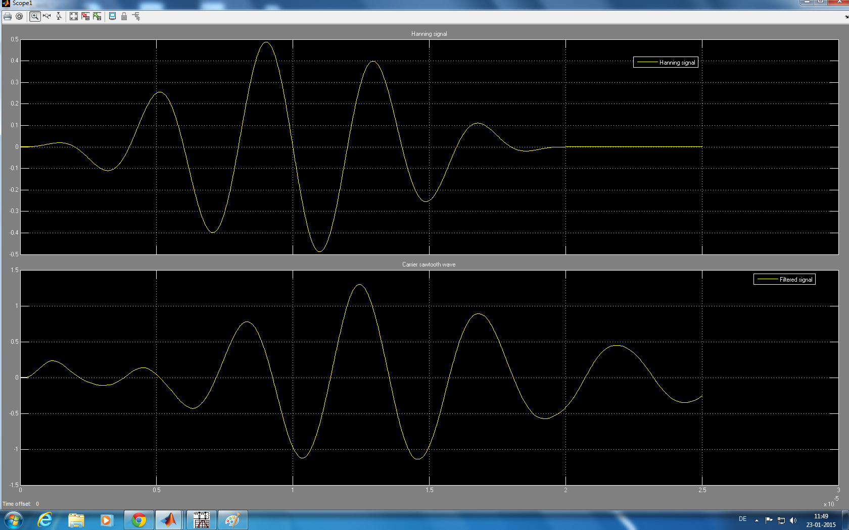
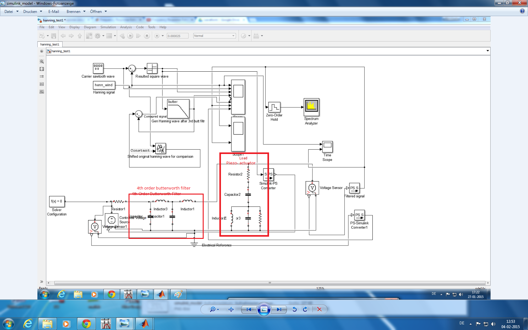
I am designing a passive analog filter for Digital to analog conversion. But i am stuck at one point. My load is not purely resistive. Actually i have to drive a piezo with my circuit. Piezo is an inductive and capacitive load. I don't have any idea about how to design filter for such kind of load. Could anyone tell me the possible method or some kind of tutorial?
 

I suggest you add an amplifier after the filter to drive the piezo load and isolate the load from the filter.
Designing a passive filter to drive a complex load would be, well, complex especially since the load probably varies with the operating conditions.
 

This option i have thought before. But the problem is i have very strict power requirement therefore i am using class-D amplifier before filter circuit as it has efficiency up to 90%. If i am designing analog amplifier than i will have maximum 50% efficiency which is not desirable. Again some distortions will be there because of switching time of FET.
 

Full featured filter design programs like Nuhertz support frequency dependent complex termination for passive filters. As you might guess, an intended filter prototype can be only implemented over a restricted termination range.

The methods for matching complex impedances or either filter element tuning for minimal error or adding compensation networks of selectable order.
 

For <10% load regulation, the source impedance must be <10% of the load at the desired frequency band.

If you don't know either the DAC driver impedance nor the piezo impedance, then how did you design your interface filter?

A 2 port passive filter can be made of series or parallel elements to give low or high impedance in either the pass or reject band.

If not sure , ask for what I assume you need to know, and give details of parts and geometry.
 

If you are just filtering the Class-D PWM frequency then the filter is not critical and you likely just need a series inductor large enough to filter the fundamental with the pizeo capacitance and motional resistance as the inductor load.
The best inductor value may have to be determined experimentally.

I have tried to simulate my circuit in simulink using only one inductor. But it cant eliminate high frequency component of signal.

- - - Updated - - -

For <10% load regulation, the source impedance must be <10% of the load at the desired frequency band.

If you don't know either the DAC driver impedance nor the piezo impedance, then how did you design your interface filter?

A 2 port passive filter can be made of series or parallel elements to give low or high impedance in either the pass or reject band.

If not sure , ask for what I assume you need to know, and give details of parts and geometry.

As of now i m silulating my circuit in simulink. So for simulation purpose i have taken source resistance as 1 ohm. I am using electrical equivalent model for piezo(Image attached). In my model i have series and parallel circuits with R,L and C. So I have calculated resultant impedance by solving circuit and it came around 79 ohms. So i have put my load resistance as 79 ohm and i have designed analog filter based on that criteria. Is my method is correct? Because i have just calculated resultant impedance but i aven't done anything with phase angel. When i simulated my circuit i got a wave form which is shifted from original(Image attached) . What should i do to avoid such things and again it doesn't resembles with original waveform.
 

You didn't give any details about base band and pwm frequency, cut-off frequency and intended attenuation. So I can only answer very generally:

A low-pass filter must be expected to involve a phase shift (respectively delay).
 

You didn't give any details about base band and pwm frequency, cut-off frequency and intended attenuation. So I can only answer very generally:

A low-pass filter must be expected to involve a phase shift (respectively delay).
Actually my aim is to generate 250KHz hanning wave signals using microcontroller and low-pass filter. PWM frequency would be 2Mhz. So cutoff frequency of filter is 250kHz and stopband frequency is 300Khz with 30db attenuation. In my last post i have uploaded the waveform generated by my designed filter. But it is not exactly same to the intended waveform i want. What can i do to avoid phase delay and make it exactly as the original one?
 

Strictly speaking that's not possible. At least a certain delay can't be avoided. But you have additional waveform distortion by a too low filter cut-off frequency.

- - - Updated - - -

I forgot to mention a point. The piezo transducer itself acts as a resonator, the waveform distortion can happen also without a filter.
 

In audio work, there is an amplifier parameter called damping. It is important because it measures the amplifier's capabilities of damping the motion impedance of a loudspeaker or transducer (in addition to electrical impedance).
 

[Moved]Compex load in Butterworth analog filter design.

I am designing butterworth filter for digital to analog conversion. Finally i have to drive piezo-actuator. Piezo is a complex load and i have electrical model for it. I already have design a filter which gives me desired frequency response when i simulate with resultant calculated real load value.(Resultant impedance of my piezo electical model). But when i put whole piezo model as complex load, it gives me some weird result. I don't know why it happens. Should i add impedance matching network or something as i am driving complex load. In attachment, "Bode_plot_with_impedance" is a resultant bode with orignal complex load and "Bode_plot_with_r" is a resultant bode with only final real load.
 

Attachments

  • Bode_plot_with_impedance.png
    Bode_plot_with_impedance.png
    15.6 KB · Views: 101
  • Bode_plot_with_R.png
    Bode_plot_with_R.png
    14.4 KB · Views: 68

You should show the circuit including the piezo model for clarity.

Generally speaking, a result like this is pretty expectable. You have apparently a piezo resonance frequency near the low-pass cut-off and it will surely appear in the overall transfer characteristic.

If the piezo resonances are far-off you could probably compensate the transducer reactance in filter design. But compensating the resonances itself is almost unrealistic.
 

I have attached the circuit which shows the filter and my complex load. My question is how to compensate transducers reactance? means should i calculate the resultant impedance of the load in the form of R+jX? If yes, than how to design compensating network for it? I am new in this field so don't have too much idea relating to this.
 

Specifying load impedance as R + jX versus frequency would allow to consider it in filter design, e.g. with Nuhertz Filter Solutions. The corrected filter can be only an approximation of the ideal transfer function, the stronger the frequency dependency is (respectively the higher the transducer Q), the worse the result.

Can you tell what's the transducer resonance frequency?
 

My peizo has two resonance frequency because series and parallel structure of circuit.
Actually my problem is little bit different now. I have already implemented filter circuit for digital to analog conversion and tested with my PWM signals(2Mhz) from microcontroller. My configuration is
Microcontroller(PWM) --> Class-D amplifier(PWM) --> 4th order butterworth filter.
I have modulated my sawtooth wave(2Mhz) with 250Khz hanning wave signal in order to get PWM waveform in simulink and than i have loaded all the data in microcontroller. I am able to filter out 250Khz output after filter but it has too much distortion and noise. I think 2Mhz sampling frequency is still present at the output. (waveform attached)


How to get rid of this high frequency in output? is it happening because of few points in PWM only? I am applying only 8 pulses of PWM for one period of hanning window.
 

How to get rid of this high frequency in output? is it happening because of few points in PWM only? I am applying only 8 pulses of PWM for one period of hanning window.
It's difficult to recognize on the low resolution oscilloscope screenshot if the high frequent signal is 2 MHz or something else. I'm sure you can see this with suitable oscilloscope settings.

It may be easier to filter the measured signal than the PWM output.

Too few points can result in distorted base band signal but won't increase PWM residuals.
 

To check for scope measurement error, probe the same signal and expect flat line on Ch1-Ch2.
If not, shorten probe grounds and calibrate probe trimcap until matched.

If 2MHz rejection is insufficient, test frequency response of filter with f sweep from 1 to 3MHz and PWM sweep from 200 to 300KHz.
Are you expecting 250KHz sinx/x to be >30dB SNR in differential mode? For phase control , I think some prefer Raised Cosine filtering.
 

Status
Not open for further replies.

Similar threads

Part and Inventory Search

Welcome to EDABoard.com

Sponsor

Back
Top