Continue to Site

Welcome to EDAboard.com

Welcome to our site! EDAboard.com is an international Electronics Discussion Forum focused on EDA software, circuits, schematics, books, theory, papers, asic, pld, 8051, DSP, Network, RF, Analog Design, PCB, Service Manuals... and a whole lot more! To participate you need to register. Registration is free. Click here to register now.

SIM900 returning "+CPIN: NOT INSERTED" and "+CPIN: NOT READY"

Status
Not open for further replies.

Sharagim

Advanced Member level 4
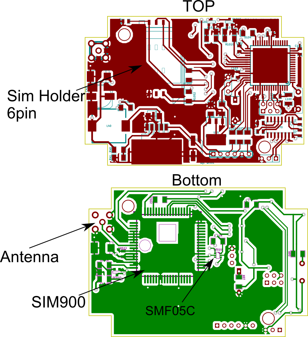
Joined
Feb 6, 2011
Messages
112
Helped
0
Reputation
0
Reaction score
0
Trophy points
1,296
Activity points
2,058
Hi,
I am developing a SIM900 board.
When I power it up most of the times I see "+CPIN: NOT INSERTED" and "+CPIN: NOT READY" a few times which it goes ready, after I make a call with ATD I see it wont response for a few seconds and then failed again. I became suspected to ESD protection of SIM Holder which is a "SMF05C" so I removed it and problem gone.
Is there any idea what is making this problem ?
 

Can happen with bad circuit layout when SIM card lines pick up too much RF.
 

Thx for your reply,
BRD attached could you please give me some advise about it? is there any problem?
 

Hi again,
Sometimes I am seeing continuously these lines(My power supply is lm2576 with two 470uf Tant+1000uf Elec):
+CPIN: READY
Call Ready
IIII
RDY
+CFUN: 1
+CPIN: READY
Call Ready
IIII
RDY
+CFUN: 1
 

Hi Again,
I tried to find out how the last problem occurring and I see when I use small antenna this is happening much more and it depend to position of antenna too. So it seems it is RF effect on circuit.
In the circuit there is polygon, is there any other ideas to decrease this effect ?

BR,
 

I see when I use small antenna this is happening much more and it depend to position of antenna too. So it seems it is RF effect on circuit.
I agree with the conclusion. But there's no simple solution for a two-layer board.

The ground pours are more or less fragmented. You can make it a bit more continuous by adding vias connecting bottom and top side ground pours. It may also help to add small RF blocking capacitors (a few pf) between the SIM signal contacts and ground or possibly series ferrites near the card holder, cutting the signal trace antenna effect.
 

Status
Not open for further replies.

Similar threads

Part and Inventory Search

Welcome to EDABoard.com

Sponsor

Back
Top