Continue to Site

Welcome to EDAboard.com

Welcome to our site! EDAboard.com is an international Electronics Discussion Forum focused on EDA software, circuits, schematics, books, theory, papers, asic, pld, 8051, DSP, Network, RF, Analog Design, PCB, Service Manuals... and a whole lot more! To participate you need to register. Registration is free. Click here to register now.

[SOLVED] What happen when use a FF triggered by falling edge of the clk?

Status
Not open for further replies.

nervecell_23

Member level 1
Joined
Apr 26, 2013
Messages
38
Helped
0
Reputation
0
Reaction score
0
Trophy points
1,286
Activity points
1,565
Hello, I've got two questions about using ff triggered by falling edge of the clock:

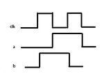
1) As shown in the figure, if I use both signal a and b to drive the same circuit that is also synchronised to 'clk', is 'a' more stable than 'b'? (Here stable I mean glitch-free)

2) How should I analysis timing for signal 'a'? I mean, for signal 'b', I've got a margin of roughly one clock cycle to accomodate combinatorial logic to avoid timing violation, but for signal 'a', do I only have half-clock cycle to play with if the signal that drives signal 'a' is synchronised to rising edge of the clock?

Thanks.
 

You forgot to include the figures to your homework quesiton..
 

You forgot to include the figures to your homework quesiton..
uh..sorry..30mins passed, I can't edit the original post, here's the figure. But since you easily figured out it's a homework question, it shouldn't be difficult for you to understand the question without the figure right :)?
p1.jpg
 

1. where do a and b come from? you would never use A is it is clearly from another clock domain
2. Dont use A at all.
 

you would never use A is it is clearly from another clock domain.

Could you clarify this, why do you think 'a' is clearly from another clk domain? Isn't it also possible to get signal 'a' by delaying signal 'b' for half cycle (using FF triggered by falling edge of 'clk', is it correct?).

As I mentioned in the original post, both 'a' and 'b' are registered signals from the output of the same combinatorial logic, both signals are used to drive the same fan-out. Could you explain why not to use 'a' at all? Is it because registered signal triggered by falling edge of the clock is not recommanded? Or is it because it is not helpful at all in sense of signal stabalisation/glitch-free consideration? Or is it because using 'a' can cause timing issue?
 

A is not on the same clock domain as it is delayed by half a clock. Doing this and then using A inside an FPGA would be poor design practice, as everything should be aligned with the clock (as B is).

This question seems a little odd, as skewing signals manually in a design to try and meet timing is never recommended. You would clock everything with the same clock as much as possible. If clock domain crossing is required, you would use safe clock crossing techniques (ideally a dual clock fifo) with appropriate timing constraints. Trying to teach you otherwise is poor teaching.
 

Reviewing this thread, I neither see a clear description (preferably a schematic) how the signals in post #1 have been generated nor a clear question.

Nevertheless I agree with the general design guidelines by TrickyDicky.
 

As you mentioned it's a homework question ... you might concider writing down your own thoughts.

If it was a professional problem - I should concider a timing simulation.
 

Reviewing this thread, I neither see a clear description (preferably a schematic) how the signals in post #1 have been generated nor a clear question.

Nevertheless I agree with the general design guidelines by TrickyDicky.
This question does not involve any specific circuit design since it's just a general question in my mind regarding designing practice. But here's a revised question:

If signal a and b are registered outputs of the same combinatorial logic, one is positive triggered and the other one is negative triggered, both signals will drive ....say a local interface of a DDR controller at the second rising edge of the clk in the figure. Will signal a be more glitch-free than b? (Since TrickyDicky suggested that using negative triggered ff in this case was a bad idea at the first place, then the answer would be NO right?)
 

Registered outputs don't show glitches. If the setup and hold requirements of a FF aren't met, it can either latch a wrong signal state or, in rare cases, fall into a metastable state with finite lifetime, from which it recovers to a stable state. That's not a glitch.

It has been already said that it's usually not helpful to latch signals on both edges of a clock in internal logic. It may be necessary for external interfaces, e.g. with double data rate processing.
 

Returning to your original questions:
1) As shown in the figure, if I use both signal a and b to drive the same circuit that is also synchronised to 'clk', is 'a' more stable than 'b'? (Here stable I mean glitch-free)

2) How should I analysis timing for signal 'a'? I mean, for signal 'b', I've got a margin of roughly one clock cycle to accomodate combinatorial logic to avoid timing violation, but for signal 'a', do I only have half-clock cycle to play with if the signal that drives signal 'a' is synchronised to rising edge of the clock?

Given two circuits like this where the top circuit has a intermediate falling edge FF and the bottom circuit has a rising edge FF.
Capture.PNG
The timing paths associated with register A will require that the setup/hold time between InA to A and between A and OutA must be met for the circuit to operate correctly. This means in both cases the paths will have to meet a setup/hold with half the clock period available. (rising-to-falling and falling to rising)

For the bottom circuit the timing paths have the entire clock period to make timing for both InA to A and A to OutA. This circuit though will operate differently than the first circuit as it takes two clock cycles to get the equivalent output.

The first circuit could also be implemented as (removing the falling edge FF entirely):
Capture.PNG
In this case the circuit now combines the two combinational blobs into a single blob, that has to meet the setup/hold requirement between InA to OutA. This circuit is functionally identical to the circuit with the falling edge FF as the input and output will be the same between the circuits. As the circuits produce the same results there is absolutely no reason to add an additional negative edge pipeline FF in the path.

Note that none of these circuits are "glitchy". For any of these circuits to work they all must meet the setup/hold time of the FFs. Yes the combinational logic may have glitches prior to meeting the path setup/hold time, but during the FF capture window (from the start of the setup time to the end of the hold time) the input to the FF must be stable, otherwise the FF may go metastable (is this what you're thinking of when you say glicth?).

As FvM stated nicely in #10 FFs don't glitch. Though some older bipolar based logic families could produce runt pulses, but today's high speed CMOS logic this doesn't occur.
 
  • Like
Reactions: Samran

    Samran

    Points: 2
    Helpful Answer Positive Rating
Status
Not open for further replies.

Part and Inventory Search

Welcome to EDABoard.com

Sponsor

Back
Top