Continue to Site

Welcome to EDAboard.com

Welcome to our site! EDAboard.com is an international Electronics Discussion Forum focused on EDA software, circuits, schematics, books, theory, papers, asic, pld, 8051, DSP, Network, RF, Analog Design, PCB, Service Manuals... and a whole lot more! To participate you need to register. Registration is free. Click here to register now.

Schematic circuit xenon lamp

Status
Not open for further replies.

tnnedaboard

Member level 3
Joined
Apr 5, 2012
Messages
64
Helped
0
Reputation
0
Reaction score
0
Trophy points
1,286
Activity points
1,748
hi

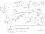
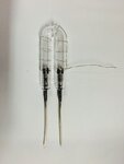
I'm trying to repair an appliance for hair removal that uses a xenon lamp. (see attached)

Such devices called IPL, activate and deactivate the capacitors to discharge at predetermined time intervals, in order to have an effect of the pulsed light flashes and available energy in the shortest time.

I made the schematic but I can not understand the function of some signals, because the microprocessor control board is broken!

is just the functioning of PIN16 - PIN20 connector CONN1 ? (see attached diagram)
Best Regards
IMG_5498.JPG

ALI_IPL_TEST.jpg
 

I can read your schematic much easier than the Italian, so I learnt some new words.

pin
20 = Logic "1" e.g. from 470 Ohm to 5V (or 330 OPhm to 3V) = AC Power ON relay
19 = Logic "1" low impedance ... Triac Phase control ( 10us min) for Pwr levels
18 = Logic "1" low impedance ... Xenon IGBT Fire enable
17= Logic "1" low impedance ... Xenon Flash Arm (Cap charge)

This is what I would call the signals above

Low impedance logic is 50 Ohm or less. and may bipolar or open for Logic "0"

Pin 12 = jumper to ground for safety flash off OFF. for debug
 

You are a great! Thanks.

is the pin16?

So the sequence of the pin to output the flash lamp?

Thanks again.

- - - Updated - - -

Excuse me,

here is the translation of the PIN in the wiring diagram:

PIN16 = active download trigger transformer for triggering
PIN17 = ???
PIN18 = active discharge capacitors
PIN19 = PWM to adjust the charge of the capacitors
PIN20 = active charging capacitors
 

Timing requires more study but the ARM or Charge input grounds the caps for charging and then released just before firing the trigger. So these are sequential.

The Phase control of the triac uses the load resistors to get some transfer function of time before zero crossing of 120Hz that increases phase advance and charge voltage on caps and thus 5 different power levels from user input selector. So some AC line clock ZCS pulse needs to be created and a variable 1 shot to increase time and decrease power or Triac ON time. up to 1/2 cycle

Was it an effective product as claimed? How long did it run before failing?

I wonder if the stray EMI pulses ( and poor shielding or filtering) or ESD caused the uC board failure.
 

Please apologize me but I didn't well understand the sequence. Is it correct the following one?:
1. Active PIN20
2. Active PIN18
3. Active PIN16
Please confirm.
I don't understand the PIN17 function yet. Could you tell me more details about it? Awaiting your reply and thanks for your collaboration
 

I'm sorry I'll explain....

ok regarding:

The Phase control of the triac uses the load resistors to get some transfer function of time before zero crossing of 120Hz that increases phase advance and charge voltage on caps and thus 5 different power levels from user input selector. So some AC line clock ZCS pulse needs to be created and a variable 1 shot to increase time and decrease power or Triac ON time. up to 1/2 cycle

but what about the sequence:
1. Active PIN20
2. Active PIN18
3. Active PIN16

And the function of PIN17?
Can serve the pin17 (and therefore T2 and RL1) to discharge the capacitors when you want a lower VCC ???
 

Hi,
and happy new year ...

Additional help, thanks ...
 

Status
Not open for further replies.

Similar threads

Part and Inventory Search

Welcome to EDABoard.com

Sponsor

Back
Top