darrylcapulla
Junior Member level 1
- Joined
- Dec 15, 2014
- Messages
- 19
- Helped
- 0
- Reputation
- 0
- Reaction score
- 0
- Trophy points
- 1
- Location
- Pili, Camarines Sur, Philippines
- Activity points
- 145
Hello Engineers,
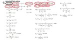
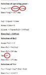
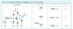
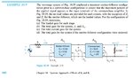
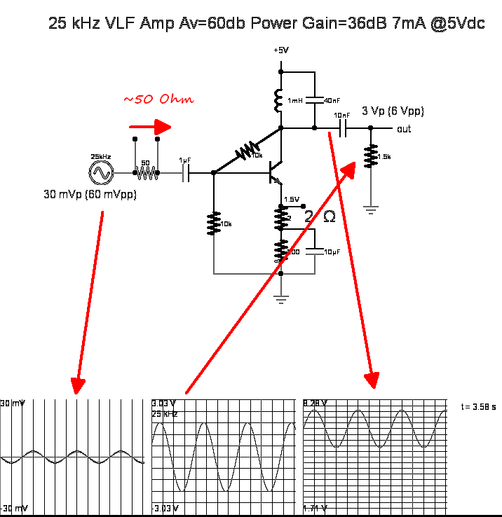
I just want to Design a Cascade BJT Amplifier Two Stages,
but my problem is, Im only given two values Vin = 50mVp @ 25Khz and Vo= 3Vp,
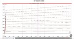
I dont really know where to start.. They say that i need to draw a transfer curve to find the Value of Ic.
Please Help me.
I just want to Design a Cascade BJT Amplifier Two Stages,
but my problem is, Im only given two values Vin = 50mVp @ 25Khz and Vo= 3Vp,
I dont really know where to start.. They say that i need to draw a transfer curve to find the Value of Ic.
Please Help me.
Attachments
Last edited by a moderator: