Continue to Site

Welcome to EDAboard.com

Welcome to our site! EDAboard.com is an international Electronics Discussion Forum focused on EDA software, circuits, schematics, books, theory, papers, asic, pld, 8051, DSP, Network, RF, Analog Design, PCB, Service Manuals... and a whole lot more! To participate you need to register. Registration is free. Click here to register now.

h bridge Switching effects the battery supply

Status
Not open for further replies.

LOSTISLAND

Member level 3
Joined
Jun 8, 2010
Messages
54
Helped
6
Reputation
12
Reaction score
5
Trophy points
1,288
Activity points
1,682
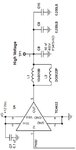
I utilize the attached circuit and the switching part is working correct
but it effects the battery supply (+12v) and drops it to 10v in minimum case of switching and brings it up to 14v in maximum one

I know if I utilize another power supply for h-bridge part other than the digital part which produces PWM , the problem is solved
But how can I use just one power supply and the problem would be solved

Thanks in advanced
 

Attachments

  • Untitled.jpg
    Untitled.jpg
    29.6 KB · Views: 132

To reduce load on battery L1, L2 impedance must be high at the applied load DC current.

L1 is 10uH is reduced by L2 in parallel which has no value given. switch rate is not given and understand you cannot solve without knowing/sharing these parameters.
 

Batteries are kind of slow to step current, and your local
decoupling appears trivial (100nF - barely enough for a
10% ripple driving a 10nF gate load even if there are no
other wasters of switching current).

On a fairly simple 10A buck converter we had hundreds
of uF worth of tantalums paralleled with multiple 47uF
ceramics and 0.1uF ceramics. So I think your decoupling
is kind of a joke unless there's way more inside the symbol.
 

Untitled2.jpg
Thanks
This is the circuit of power supply
The carrier frequency is 125 khz and the output voltage is 300v peak to peak
I seperated the +12v of the digital parts of the board including the micro-controller which generates the PWM with the +12v of the tc4422 but the problem persists yet !!!!!

- - - Updated - - -

I found something ,
The GND of the power supply which I use has difference to 5 volts with the GND of the board
In fact the sin wave (125 khz) is seen between the 2 GNDs
May be the magnetic field which is produced by the LF coild is effecting the wires which supply the board ?
 

Ok looks like your LC values do not match the applied f.=1/(2pi sq.rt(LC)
Q gain depends on L/Rs at resonance.

-below resonance , current will increase as f is reduced, causing battery voltage to drop.
 

I connected the ground of the tc4422 dirrectly to power supply and disconnected it from the digital part of the board and the problem got solved
It seems the reverse current from the tc4422 which flows back to digital part was the problem

Now another point
When I disconnected the +12v and GND of tc442 from the digital part and connected them directly to power supply , the board worked fine for some time
but the tc4422 corrupted
When cutting the VCC and GND , the capacitor and diode which was common in digital and tc4422 was remained in the digital part and power supply dirrectly connected to the tc4422 circuit
Exactly the same as the picture in my first post
Can this corrupt the tc4422 ?!
 

Your TC4422 is driving a 12V square wave into a series resonant circuit, which can be almost a short circuit. Now this chip has a long term 1.5A current limit and a power dissipation limit. There is no thermal shut down protection. So basically you must put a low value resistor in series with the output to limit the current and monitor the temperature of the chip to make sure it does not get too hot (or put it on a heat sink).
Frank
 

The tc4422 was not working for more than 3 seconds and it was corrupted
I don't know why
maybe feedimg PWM while +12V was not yet stable caused the problem ?
 

which power switch you are using in H-bridge circuit ..
as for example if you are using Mosfet you need Isolation between Your power circuit and control circuit other wise your Ground short your Lower arm of H-bridge....

so for Mosfet you must use Mosfet driver....
 

What do expect this circuit to do other drive a <10A , 10Vpp square wave into a low pass filter?

Again I ask what is this for?

You can control the impedance at series resonance and amplify the voltage at the expense of current at series load impedance. The gain or Q is the ratio X(f)/Rs at resonance. Gain reduces with Load resistance as well to a Q=1 when matched to impedance at resonance.

Discussion is pointless without purpose.
 

This is generating LF signal (300v p2p) and a receiver would receive this wave and demodulates to get data out of it
I don't know why the mosfet driver failed yet
inductive kickback which has damadged the low side driver of tc4422 ?!

- - - Updated - - -

What can I do for the inductive kickback ?
This circuit is designed by a well known company (I don't say what it is cause this site is Atmel board)
How can I find a circuit which is industrial and working properly ?
 

Thanks
I'm working to find an industrial driver
 

Status
Not open for further replies.

Similar threads

Part and Inventory Search

Welcome to EDABoard.com

Sponsor

Back
Top