Continue to Site

Welcome to EDAboard.com

Welcome to our site! EDAboard.com is an international Electronics Discussion Forum focused on EDA software, circuits, schematics, books, theory, papers, asic, pld, 8051, DSP, Network, RF, Analog Design, PCB, Service Manuals... and a whole lot more! To participate you need to register. Registration is free. Click here to register now.

LC filter design for converter

Status
Not open for further replies.

sam781

Full Member level 4
Joined
Oct 22, 2011
Messages
212
Helped
7
Reputation
14
Reaction score
7
Trophy points
1,298
Activity points
2,757
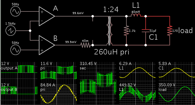
I'm trying to make a full bridge converter having the following parameters -

Input nominal voltage = 12v
PWM frequency=80kHz
Transformer turns ratio =34

Expected output dc voltage = 12*34*0.8=326v [duty cycle 80%]

Now, to get the expected dc voltage, I want to calculate required inductance and capacitance to make LC filter. I've read some post but still not clear about the calculation.
Ripple voltage and current can be taken as 1% and 10% respectively. What equations should I consider for L and C?
 

It depends what topology is used. Half bridge resonant or full bridge flyback or feed forward. Square wave, tri-level , pseudo-sine wave

one must also consider egress noise for total filtering of CM and DM filters and define those falong with output harmonic content.

But normally operating any bridge is at 2x fundamental frequency, if single phase with PWM increasing harmonic factors.

The impedance at SRF needs to be compared with equivalent load for startup and steady-state, where Z=P/I^2. The impedance divider ratio determines ripple voltage. The ESR factors into startup current and ripple current as well as load reactance and nonlinearity if no PFC is included.

More design specifics needed on topology, harmonic content , load impedance etc.

Synchronous PWM inverters have improved harmonic content. Nxf
 

By 'full bridge converter' you imply AC, correct?

Ballpark values can be gotten by using the formula for capacitive and inductive reactance.

XC = 1/ (2 Pi f C)

XL = 2 Pi F L

You want X values to be in the vicinity of your load resistance.

By changing the ratio of L-to-C, you can raise or lower your output voltage.
 

It depends what topology is used. Half bridge resonant or full bridge flyback or feed forward.
Full bridge -
converter-inverter.png


one must also consider egress noise for total filtering of CM and DM filters and define those first.
I think I should consider Continuous Mode (CM) filter which is better for my application. Don't know where and why DM is required.


But normally operating any bridge is at 2x fundamental frequency, if single phase with PWM increasing harmonic factors.
Why it is 2x of fundamental frequency?


The impedance at SRF needs to be compared with equivalent load for startup and steady-state, where Z=P/I^2. The impedance divider ratio determines ripple voltage. The ESR factors into startup current and ripple current as well as load reactance and nonlinearity if no PFC is included.
I want to get around 300-350w from the final inverter output. So, load impedance should be somewhere around 150-175 ohm.


More design specifics needed on topology, harmonic content , load impedance etc.
Overall high level design diagram has been shared above for your comment.


Synchronous PWM inverters have improved harmonic content.
Want to know about it...
 

If Vdc is ideal 0 Ohm and not shared, then DM filter is not required.

disregard 2x f, was thinking of rectified load currents on enduser load from AC out.

Read up on synch inverters and pseudo sine inverters for lower harmonic content.

transformers are rated in V-s of capacity , I recall with core choice critical to,avoid thermal runaway under startup surge or overload conditions.

V t = NABpk
where Bpk is the peak flux density and A is the core area. For a given period, t ,
voltage, V , and maximum flux density Bsat , an N.A product may be found
 

@BradtheRad
I've uploaded a hihg level design diagram for better understaing. Please let me know if more info is needed to get the required value of L1 and C1.

@SunnySkyguy

I've sorry; I'm not getting the point you are trying to make me understand... It would be great if you could explain a little more or share links on the following topics-
synch inverters
pseudo sine inverters
transformers are rated in V-s of capacity
 

From my experiments with a simulation, it becomes evident that L1 & C1 have a big effect on waveforms in the primary loop. Apparently their values should be chosen for the 50 Hz fundamental frequency.

Notice the 'pri. volts' and 'pri. amperes' waveforms in the screenshot. They are pretty much in alignment. This is necessary to proper operation of the inverter. The issue is power factor correction.

However if L1 or C1 are changed much, one waveform shifts forward or backward. This makes for inefficient power factor.


The carrier frequency is 1.5 kHz. Some values may need to be changed since your carrier is 80 kHz.

I can see there is some inefficiency, as far as watts in vs watts out. I tried to improve it, but that will take more know-how and experimentation.
 

@BradtheRad

Transformer's input waveform (80kHz) screenshot is attached herewith. Note that I want to make 326v dc from transformer's output. I missed bridge rectifier section which should be placed between transformer's output and the LC filter. Sorry for the inconvenience...

Could you please let me which simulation application you have used?

- - - Updated - - -

20141203_215924-1.jpg
80kHz PWM waveform after connecting Bridge output to Transformer's primary.

- - - Updated - - -

Transformer info -

Core ETD39
PWM frequency=80kHz
Transformer turns ratio =34
Turn per volt = 0.25
Primary turns = 4
Secondary turns =136
Transformer input voltage=12v
Transformer output voltage=408v
 

@BradtheRad
Could you please let me which simulation application you have used?

This is Falstad's animated interactive simulator. Free to download and use at the link below. You need to have Java installed on your computer.

www.falstad.com/circuit
 

Thanks BradtheRad for sharing the link of interactive simulator. I'll check it...

Could you please help me claculatiing the required L and C for my converter? Transformer input waveform and some more relevant info has already been given in the earlier posts.
 

Thanks BradtheRad for sharing the link of interactive simulator. I'll check it...

Could you please help me claculatiing the required L and C for my converter? Transformer input waveform and some more relevant info has already been given in the earlier posts.

It just so happens, your LC low-pass filter resembles a woofer crossover, second order butterworth.

Calculator for speaker crossovers:


You'll get different results depending on load and frequency. A reasonable cutoff frequency is 80 Hz. (I used 79 Hz and 28 ohms in order to match my simulation values above.)

To get a particular voltage at your load, play with the L:C ratio.
 

You usually won't place a LC filter between the rectifier and the DC bus of the inverter output stage.

The high voltage DC bus however needs bus capacitors. They won't be selected using low pass design formulas, instead 100 Hz ripple current and respective ripple voltage determine the selection. You want to keep the 100 Hz load pulsation inside the output stage and don't pass it to the DC/DC converter.

A series L between rectifier and bus capacitor may be useful if the DC/DC converter utilizes PWM to control the output voltage or to reduce peak currents. Also the inductor value would be selected according to current ripple rather than low-pass design criteria.

A low-pass filter for the output inverter is suggested if it uses sine pwm, it's rarely used for a square wave inverter.
 

I agree with FVM, which gets back saturation effects of any core used in pulse mode, transformer or filter.

transformers are rated in V-s of capacity , I recall with core choice critical to,avoid thermal runaway under startup surge or overload conditions.

V t = NABpk
where Bpk is the peak flux density and A is the core area. For a given period, t , and voltage swing V.


Look at core specs or choke or pulse transformer specs.
 

I've generated 80kHz output from MOSFET bridge and the transformer is not getting saturated. Transformer connected to the bridge output seems okay so far...

Now, I need to have at least 326v DC. Need to know how can I get this?
 

I've generated 80kHz output from MOSFET bridge and the transformer is not getting saturated. Transformer connected to the bridge output seems okay so far...

Now, I need to have at least 326v DC. Need to know how can I get this?

You are missing alot of details in the design like leakage inductance in the transformer, phase shift, synchronous switch gate design etc and you wish to design LC in the wrong place !! LC is post secondary.

You have a lot to do before this question can be answered.

Here is one example fully explained.
https://www.vishay.com/docs/69747/answitch.pdf
 

A full diode bridge is how you can turn AC into DC. Following that, a smoothing capacitor rated for over 330V.

I have to say it isn't clear any more, whether you want the final output to be AC or DC? My replies were from the notion you want AC sinewaves.
 

A full diode bridge is how you can turn AC into DC. Following that, a smoothing capacitor rated for over 330V.

I have to say it isn't clear any more, whether you want the final output to be AC or DC? My replies were from the notion you want AC sinewaves.

It looks like he should use a resonant sine wave converter where LC has a Q of 1 at full load at switching rate. When the LC filter is post secondary or differential across the bridge output for a distortion free sine out with true zero crossing switching at synchronous switching rates.

Thus at full load LI²=CV² = 2x Po output power. Load step performance requires adaptive PWM and phase of PWM is critical for low harmonics of 50 Hz
 

Sorry to make all of you confused with my requirement and the high level diagram (wrong) shared earlier. I've made a revised diagram for the converter part only to make you understnad about the requirement.

The converter will convert 12 dc to 326v dc in output across C1. To get dc in the output, I need the calculaiton for the required value of L0 and C1. Load will be 1A at output.
 

Attachments

  • invrter - converter_Circuit.png
    invrter - converter_Circuit.png
    20.2 KB · Views: 108

you still haven't specified the switching rate which affects ripple. nor have you specified desired ripple level at full load. nor if the load is non-linear and it would be nice to know the transfer impedance of the transformer for Q resonance factor. But essentially LC impedance is selected at a resonant frequency and attenuation for 2 pole LPF is reaches 40dB/decade, so 1% ripple is at least 2 decades below switching rate. 10% ripple is at least 1 decade below..

RLCF nomograph helps to find quick ballpark values at the intersections of sloped values of L and C at the equivalent load impedance for a Q of 1 ( dampened) which goes to high Q with no load. meaning any input noise at this resonance gets amplified significantly (if present.) Otherwise ignore.View attachment ImpedanceNomograph.pdf
 

SunnySkyguy

Could you please give an example on how to use the nomograph.
 

Status
Not open for further replies.

Similar threads

Part and Inventory Search

Welcome to EDABoard.com

Sponsor

Back
Top