Continue to Site

Welcome to EDAboard.com

Welcome to our site! EDAboard.com is an international Electronics Discussion Forum focused on EDA software, circuits, schematics, books, theory, papers, asic, pld, 8051, DSP, Network, RF, Analog Design, PCB, Service Manuals... and a whole lot more! To participate you need to register. Registration is free. Click here to register now.

Virtual Ground between Switches

Status
Not open for further replies.

BKI

Member level 1
Joined
Jul 23, 2014
Messages
33
Helped
0
Reputation
0
Reaction score
0
Trophy points
6
Activity points
264
Hi,

i like to add a virtual ground between two Switches.
The idea is, i connect two NMOS in series connected on the source sides.
Then i want to add a virtual ground between the Switches. (see pic)

Why i need this? Because of my limitations.
Vgs,max=5V, Vds,max=300V, Vgate,max=5V, Vin=200V , Vout should be 200V.

Therefore, my Vsource should be 0V.

How can i implement this the simplest way, without using an OpAmp?

Analog Switch with Virtual Gnd.png
 

What type of MOSFET has a 300V Vds with only a 5V Vgs maximum?

You can't use a virtual ground with such a circuit. The MOSFET ground must be referenced to the 200V supply.

What exactly are you trying to switch and at what speed?
 

What type of MOSFET has a 300V Vds with only a 5V Vgs maximum?

You can't use a virtual ground with such a circuit. The MOSFET ground must be referenced to the 200V supply.

What exactly are you trying to switch and at what speed?

The MOSFET itself has a Maximum Vgs of 20V, but i only have 5V supply voltage.
I try to Switch 200V (generated from a boost converter) to a load by a control signal(0/5V).
But i always have the problem that a source voltage of 200V forces me to have a gate voltage of at least 205V.
Therefore, i through about reducing the source voltage to an acceptable Level.
Frequency is uncritical with 500 Hz. Area is very critical.

Any idea how i can switch the rail to the output?
This issue is very critical to me, as it is part of my Master Thesis that i want to finish in just a few weeks.
Please HELP!!!
 

Do you have P-MOSFETs available?
Why are you using two MOSFETs in series?

Yes, i can use external PMOS PHC2300P.

Two Mosfets because i throught of resistive divider with same resistor Rds,on to make the source Connection Zero potential.
If i use just one Mosfet, it is impossible to implement, because i always have Problems with Vgs. Then i have 200V on the source side and 5V on the gate side, which means a Vgs of -195V. No Mosfet is able to withstand this Vgs.
In your first picture, you showed both MOSFET Sources connected to the virtual ground. But stop and think about what actual voltage that virtual ground needs to achieve, with respect to true local ground. When the MOSFETs are turned on, the Source needs to be at the same potential as the Drains, which is +200v above true ground. (And the gates would also be positive with respect to those Sources so that the switches are on, so maybe +210v). When the MOSFETs are turned off, the Sources must be at the same potential as the Gates, and they must also be no higher than the Drain potential, because even when the N-channel MOSFET is turned off, it still conducts like a diode from Source to Drain. But when the switch is turned off, the load potential should be 0v. Therefore the Source potential must also be no more than 0.7v (to prevent the diode conduction).

Taking all this into consideration, we find that the virtual ground must be jumping between +200v and ~0v as the switch switches between on and off. So your Gate drive needs to be floating - perhaps optically or transformer coupled. But if you are willing to go to all that trouble, you might as well use only one MOSFET with a floating date drive and be done with it. There is no advantage to using two MOSFETs with their Sources connected.

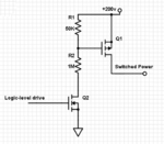
Using a P-channel MOSFET is no piece of cake either. If your switching signal originates around 0v (ground), you still have to level-shift that switching signal to up near the +200v range. You could use an open-collector NPN transistor or small MOSFET followed by a voltage divider connected to the collector/drain to generate the gate drive for the P-channel MOSFET.
 

You can use a voltage divider to drive the base. With a P-MOSFET, connect say a 50k resistor between drain and gate, and a 1 megohm resistor between the MOSFET gate and a high voltage switch to ground.
Then when the switch is turned on, grounding the 1 meg resistor, the Vgs voltage will be -10V, turning on the P-MOSFET.
Opening the switch causes Vgs to go to 0V, turning off the MOSFET.


Did i understand this correct? (See Picture)

Analog Switch Vorschlag Forum.png

Some more questions to it:

- Isn´t it better to connect the source to the Input instead of the drain? Then the Vgs is also Independent of the Output.(See Picture)

Analog Switch Vorschlag Forum 2.png

- Another important question is, isn´t it a Problem that Vg is on a unknown voltage Level when the resistor is Floating because the above MOSFET is off? An important Information to know is that the 200V are always available on the Input.
 

No, more like this:
Hi-side switch.png
But note that response time will be limited by the RC time constant formed by the 50K resistor and the (fairly large) gate capacitance of the P-channel MOSFET.
 
Last edited:

No, more like this:
View attachment 111712
But note that response time will be limited by the RC time constant formed by the 50K resistor and the (fairly large) gate capacitance of the P-channel MOSFET.

Ok, so it is how i thought with source connected to the resistor divider.

But still, isn´t it a Problem that when the NMOS is off, the gate voltage is uncertain.
Don´t you think it is better to add something to the gate node that fixes the gate node to a certain voltage Level, when the NMOS is off? Like Vgs=+10V for example?
 

No, when the N-channel MOSFET is off, the gate of the P-channel MOSFET is pulled to the same voltage as the Source by the 50K, thus turning off the P-channel. Remember, in this drawing, the Source of the P-channel is on top.
 

If the switch response time is too slow, you can reduce the resistor values (with a corresponding increase in power dissipated in the resistors, of course). If the dissipation becomes too high for the speed you need you can add a pair of complementary transistor drivers to the gate circuit.
 

Status
Not open for further replies.

Similar threads

Part and Inventory Search

Welcome to EDABoard.com

Sponsor

Back
Top