4EverYoungs.71
Junior Member level 1
Hi
I've designed a single side "dark detector circuit" in Orcad schematics and transfer the circuit to Orcad pcb boards,after arranging the components i tried to make auto rout, and i got a result which is not ok since i found that some tracks crossing each other but in circuit the are not crossed(no connected to each other) and i don't know why and how to resolve this problem.
the steps i have made for the design a single side board
1-I have drawn the circuit in schematics
2-I've mad custom pins(2 layers) to use in my components(sample of my PAD
 )
)
3-I've made my footprints for the components and used my custom pads
4-I've transfered the circuit to pcb editor
5-I setup my board dimensions and grids
6- I've setup router keep in and package keep in areas
7-since i want single side board,i have disabled the Top layer in the visibility option
8-I've opened made the auto routing window , disabled the TOP layer(since i want single side board) and made auto routing and got wrong routing results as mentioned above
is there any things wrong in my setting for the board as single side board
pls help
I've designed a single side "dark detector circuit" in Orcad schematics and transfer the circuit to Orcad pcb boards,after arranging the components i tried to make auto rout, and i got a result which is not ok since i found that some tracks crossing each other but in circuit the are not crossed(no connected to each other) and i don't know why and how to resolve this problem.
the steps i have made for the design a single side board
1-I have drawn the circuit in schematics
2-I've mad custom pins(2 layers) to use in my components(sample of my PAD
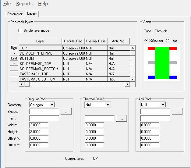
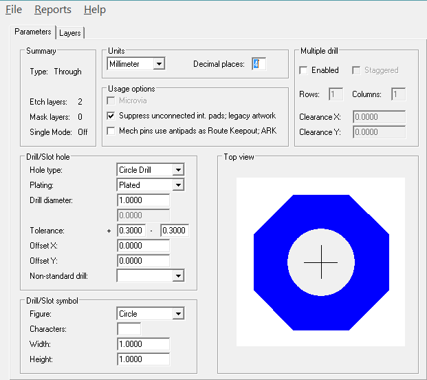 )
)3-I've made my footprints for the components and used my custom pads
4-I've transfered the circuit to pcb editor
5-I setup my board dimensions and grids
6- I've setup router keep in and package keep in areas
7-since i want single side board,i have disabled the Top layer in the visibility option
8-I've opened made the auto routing window , disabled the TOP layer(since i want single side board) and made auto routing and got wrong routing results as mentioned above
is there any things wrong in my setting for the board as single side board
pls help
Last edited: