thylacine1975
Full Member level 6
- Joined
- Dec 7, 2010
- Messages
- 337
- Helped
- 227
- Reputation
- 448
- Reaction score
- 214
- Trophy points
- 1,323
- Location
- Canberra, Australia
- Activity points
- 5,166
'afternoon all,
I've been working on a two-independently-controllable-axes motorised platform for a local charity for the past while and I've run into some difficulties with my motor driver circuits. In a moment of stupidity, I decided it would be a good idea to reinvent a brushed motor driver rather than buy a convenient module, so I opted to use Allegro's A3941 (https://www.allegromicro.com/~/media/Files/Datasheets/A3941-Datasheet.ashx) H-bridge driver IC driving 4 MOSFETs in an unimaginative datasheet-suggested configuration.
The relevant piece of the schematic is thus:
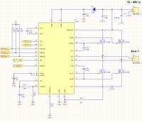
The inputs to the A3941 are driven by the open collector outputs of a PIC microcontroller (on another page) and all the digital IOs are pulled up to +5V via 10K resistors [3 are shown as R7-R9 above]. As far as I can tell, I've correctly implemented the bulk of the recommended layout considerations from the datasheet. The motors being driven are 24V brushed AEG wheelchair motors, consuming ~10A at maximum load.
My problem is that the A3941 is applying extra, unwanted switching voltages to the output FETs that a) generate lots of heat dissipation in the driver IC, b) rob the motor of any drive current and c) I can't see where they're coming from!
Allow me to illustrate...
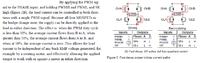
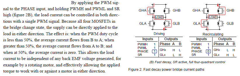
I've tried all of the operating modes (set by the various configurations of PWM_H, PWM_L, SR and PHASE) listed in the datasheet and I observe the same behaviour. For simplicity, the following pictures are for full "four-quadrant control" where the PWM signal is applied to the PHASE input pin and all other control inputs are tied high (via 10K). The excerpt from the datasheet shows what to expect:
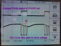
What I see is the desired PWM waveform, but "chopped up" with a higher frequency component:
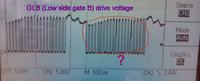
...which is also there on the gate of the FET on the other side of the bridge...
It's interesting how the applied gate voltage is 'drooping' over time - presumably as the internal charge pump struggles to keep up with the rapidly-switched gate drive requirements. While the internal charge-pump operates at a similar frequency to the observed HF chopping, they are asynchronous - I checked") The pictures were taken with the FETs unloaded (i.e. the motor absent), although the waveforms remain unchanged with a 10ohm resistive load (i.e. ~2A peak current) connected to the bridge.
The pictures were taken with the FETs unloaded (i.e. the motor absent), although the waveforms remain unchanged with a 10ohm resistive load (i.e. ~2A peak current) connected to the bridge.
Does anybody have any suggestions as to what might be going on? It doesn't appear to be an 'oscillation' of the sort able to be tamed with gate resistance (it's a deliberate, switched commutation). Varying the PCB parasitics by running my hands all over the board fail to change anything. Altering the bridge dead-time values (via the control resistor) from 1us - 5 us only slightly varied the timing but not the character of the problem. Oh, and the "problem" is present on both (independent) axes of the machine too, suggesting it's not an isolated wiring/assembly/soldering issue.
I'm pretty much out of ideas - if anyone's got an "I've seen something like this before" thought to share, please do ...before something drastic happens!
Cheers
I've been working on a two-independently-controllable-axes motorised platform for a local charity for the past while and I've run into some difficulties with my motor driver circuits. In a moment of stupidity, I decided it would be a good idea to reinvent a brushed motor driver rather than buy a convenient module, so I opted to use Allegro's A3941 (https://www.allegromicro.com/~/media/Files/Datasheets/A3941-Datasheet.ashx) H-bridge driver IC driving 4 MOSFETs in an unimaginative datasheet-suggested configuration.
The relevant piece of the schematic is thus:
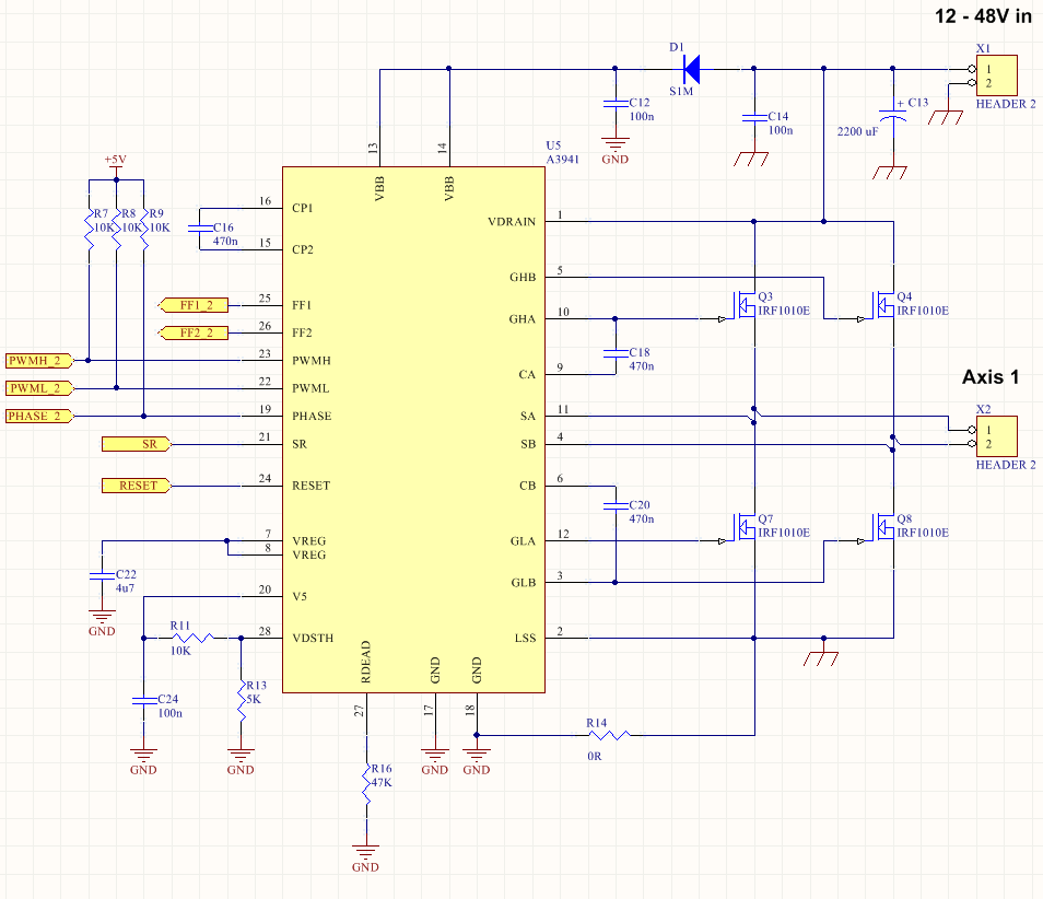
The inputs to the A3941 are driven by the open collector outputs of a PIC microcontroller (on another page) and all the digital IOs are pulled up to +5V via 10K resistors [3 are shown as R7-R9 above]. As far as I can tell, I've correctly implemented the bulk of the recommended layout considerations from the datasheet. The motors being driven are 24V brushed AEG wheelchair motors, consuming ~10A at maximum load.
My problem is that the A3941 is applying extra, unwanted switching voltages to the output FETs that a) generate lots of heat dissipation in the driver IC, b) rob the motor of any drive current and c) I can't see where they're coming from!
Allow me to illustrate...
I've tried all of the operating modes (set by the various configurations of PWM_H, PWM_L, SR and PHASE) listed in the datasheet and I observe the same behaviour. For simplicity, the following pictures are for full "four-quadrant control" where the PWM signal is applied to the PHASE input pin and all other control inputs are tied high (via 10K). The excerpt from the datasheet shows what to expect:
What I see is the desired PWM waveform, but "chopped up" with a higher frequency component:
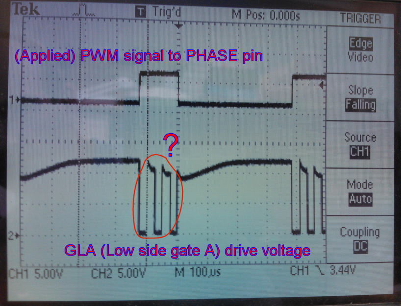
...which is also there on the gate of the FET on the other side of the bridge...

It's interesting how the applied gate voltage is 'drooping' over time - presumably as the internal charge pump struggles to keep up with the rapidly-switched gate drive requirements. While the internal charge-pump operates at a similar frequency to the observed HF chopping, they are asynchronous - I checked
The pictures were taken with the FETs unloaded (i.e. the motor absent), although the waveforms remain unchanged with a 10ohm resistive load (i.e. ~2A peak current) connected to the bridge. Does anybody have any suggestions as to what might be going on? It doesn't appear to be an 'oscillation' of the sort able to be tamed with gate resistance (it's a deliberate, switched commutation). Varying the PCB parasitics by running my hands all over the board fail to change anything. Altering the bridge dead-time values (via the control resistor) from 1us - 5 us only slightly varied the timing but not the character of the problem. Oh, and the "problem" is present on both (independent) axes of the machine too, suggesting it's not an isolated wiring/assembly/soldering issue.
I'm pretty much out of ideas - if anyone's got an "I've seen something like this before" thought to share, please do ...before something drastic happens!
Cheers