Continue to Site

Welcome to EDAboard.com

Welcome to our site! EDAboard.com is an international Electronics Discussion Forum focused on EDA software, circuits, schematics, books, theory, papers, asic, pld, 8051, DSP, Network, RF, Analog Design, PCB, Service Manuals... and a whole lot more! To participate you need to register. Registration is free. Click here to register now.

Mosfet sizing problem in charge pump using CMOS 0.18um technology

Status
Not open for further replies.

Donna Ambalong

Newbie level 2
Joined
Oct 2, 2014
Messages
2
Helped
0
Reputation
0
Reaction score
0
Trophy points
1
Location
Iligan City, Philippines
Activity points
15
I've been simulating a PMOS charge pump and my application is on non-volatile memory circuits (i.e. EEPROM). My concerns are the following:

1. What is the desired current value should the charge pump dissipate for my target application?

2. Any desired sizes for my PMOS devices to acquire the said current?

I'm using 0.18um CMOS technology
This is the circuit:
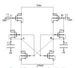
ckt.png
 

Problem on sizing pmos charge pump

I've been simulating a PMOS charge pump using 0.18um CMOS technology via SYNOPSY. The problem is all the PMOS devices are in cut-off region when extracted the .lis file and I have to drive a current of 10uA for EEPROM as an application. But when I tried to increase the sizes of the PMOS devices the output voltage seems to go down from the desired output voltage. What could be the problem or any idea how should this be solved?
Refer to the figure below for the circuit:
Screenshot_28.png
 

Question: Since you refer to P-devices, then your schematic #2 has the correct mosfet icons. However they still have a connection from the gate to the lower terminal. Did you intend this?
 

Status
Not open for further replies.

Similar threads

Part and Inventory Search

Welcome to EDABoard.com

Sponsor

Back
Top