Continue to Site

Welcome to EDAboard.com

Welcome to our site! EDAboard.com is an international Electronics Discussion Forum focused on EDA software, circuits, schematics, books, theory, papers, asic, pld, 8051, DSP, Network, RF, Analog Design, PCB, Service Manuals... and a whole lot more! To participate you need to register. Registration is free. Click here to register now.

[SOLVED] 48V PWM Inverter With MOSFET Switch

Status
Not open for further replies.

mcmsat13

Member level 5
Joined
Apr 24, 2013
Messages
94
Helped
4
Reputation
8
Reaction score
4
Trophy points
1,288
Activity points
2,287
Please I need your help here. I apologise that this thread might be seen as question that one or more members have already asked but bear with me because this one is unique with many reasons.
I'm working on a 48v Inverter system, using MOSFETs as the switch. The switching topology is push-pull, 12 pcs of IRFP260N on each side. Each MOSFET has 12k on gate to source. As they are in parallel, I think this means 1k gate to source resistance?
Gate series resistor is 47R.
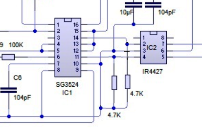
The problem is that I use a separate pair of MOSFET for testing this Inverter, one on each side, with 1k gate to source and 47R series R, still if I switch the power...boom!!! The two MOSFET blow like Christmas banger! My driver is the popular SG3524N and IR4427 MOS driver. I removed the driver and use Totem-Pole, all the same! The Oscillator/driving stage is supplied with 12v and removing the leads that go to gate, I measured;
frequency = 51Hz
duty cycle = 49.99%
voltage = 5.86V.
Remember, rail voltage is 48v which is at 54v at the moment. The trafo is a working one. It is from another working system of the same config.
I have looked at the drivers, nothing is wired wrongly! The MOS BLOW INSTANTLY AT POWER UP!
Please what else can I do?
 

You can start by putting 'scope probes to both gates and
both sources, and see whether you are turning on both at
once. All of the detail you mention, says nothing about the
goings-on.
 

post the schematic.... and check the gate waveform in the scope before applying drain voltage
 

If you have a 220V heater, connect it in series with +48V and transformer power input. This will limit current and stop fireworks and let you take further measuements.
 

Thanks to all I'll go through ur directions and see which one help.
 

Inverter Board.jpg

There is something I want to let this board know and as well ask a question; This circuit above is the circuit I use in my inverters. They have been working until I build this one, placing the components closely which resulted in small space accommodation. I have gone through the circuit and there is no component wired incorrect. All is ok but the layout is closer that those boards that work. If I connect the spaced board, this same system work, no explosion, just working. the other two boards that are closely laid out cause the MOSFETs to blow.

Now, I want to know, how does layout affect this inverter circuit. Please I have found out that it is from the circuit board I want to understand how close layout can affect the operation of this circuit.
 

If I lay out the circuit as they appear in the drawing, it works but if I lay it out compacted on a small board, even though nothing touches each other...Explosions!!!
 
I can't see any reason for this at all. It has to be something to do with the construction when made smaller. For example, are the output stage transistors isolated from each other and the heat sink?

If it checks out OK, try disconnecting both the resistors feeding the MOSFET gates (leave the ones to ground connected) and switch on. Nothing should happen and no part of the circuit should draw enough power to be damaged so you can safely check voltages for anything that looks wrong.

Brian.
 

I thank all of you for your effort. I am the poster of this thread and i don't think it will be good to leave this thread open as the problem has been solved.

Please for any younger person in this power electronics of a thing, listen...the cause of the problem that made me to start this thread is the LAY-OUT of my component in VERO board!

I laid my components tight so that they will be contained in a small space in the board. I did it and I never know that it will cause so much firework of a thing! After looking at the board, I so no mistakes, no dead component, no shorts...and still when you press the switch...Boom! I build another board, laid it out as I use to do before just as the components appeared in the circuit attached above, it worked!

I removed every components from the troubled board and built another board with them careful not to introduce another new one. I use my normal lay out just as the circuit diagram attached above. I tested it and nit also worked! No firework! I was surprise that layout can cause such a dramatic effect!

I build another new board with new components using exactly the layout of the troubled board and tested it...Boom! The sound of the blown mosfet could be hear in kilometers!

Thanks all.
 

Problem may be caused by high input impedance of IR4427. It requires only 10uA input current to switch. I recommend these two resistors to put in your faulty board and see the results.
9550143000_1413325960.png
 
  • Like
Reactions: vidal

    vidal

    Points: 2
    Helpful Answer Positive Rating
Status
Not open for further replies.

Similar threads

Part and Inventory Search

Welcome to EDABoard.com

Sponsor

Back
Top